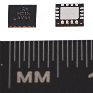
Bootloader Chip for DIY Teensy 4.0 & 4.1 Projects
| IC_MKL02Z32_T4_QFN16 | MKL02 chip with pre-programmed Teensy 4.x bootloader | $6.25 | |
|
|
IC_MIMXRT1062DVJ6B_BGA196 | IMXRT1062 chip, For DIY Teensy 4.1 Prototypes, 12mm BGA, 0.8mm pitch | $14.00 |
| IC_W25Q64JVXGIM_DFN8 | W25Q64 Winbond Flash Memory chip, For DIY Teensy 4.1 Prototypes | $1.20 | |
| IC_DP83825IRMQT_QFN24 | DP83825 Ethernet PHY chip, For DIY Teensy 4.1 Prototypes | $1.90 |
|
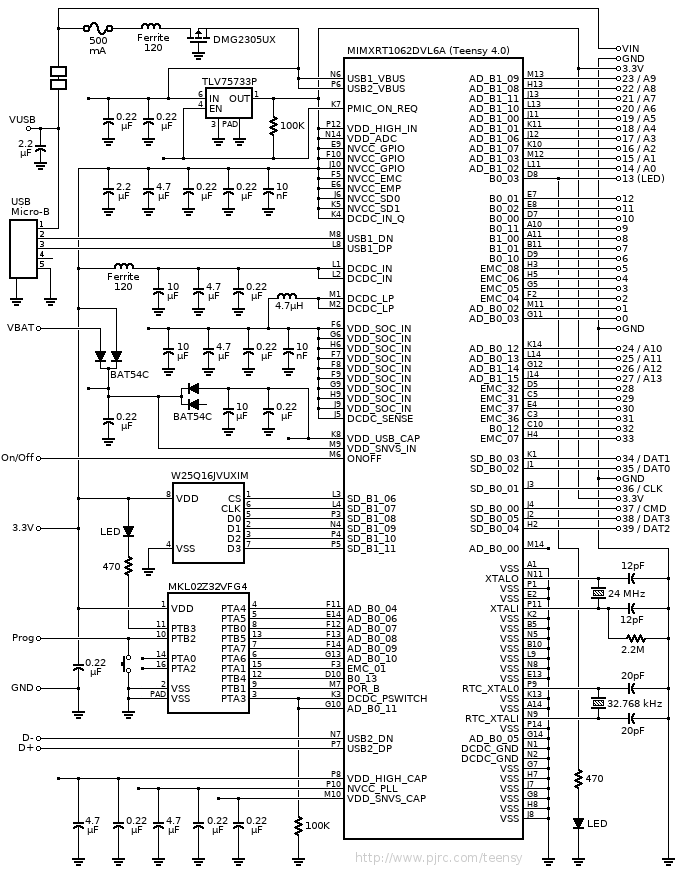
This chip, together with an IMXRT1062 microcontroller and Winbond flash memory allows you to create a DIY circuit board which is fully compatible with Teensy 4.0 or Teensy 4.1.
Supported Chips
An IMXRT microcontroller and flash memory chip must be paired with this MKL02 to form a working system. No programming or other setup is needed on these other chips. Blank chips sold by distributors are used.
- IMXRT1062DV*6B or IMXRT1062DV*6A (NXP)
- W25Q16JV*IM (Winbond)
- W25Q64JV*IM (Winbond)
IMXRT1062 chips with extended temperature range are likely to work. Success with some of these chips has been reported on the forum.
Winbond flash memory chips with a "Q" at the end of their part number do not work. Only the "M" parts are supported.
Power Up Sequence
The IMXRT1062 chip has special power-up sequence requirements. While PJRC generally recommends following the Teensy 4.0 or Teensy 4.1 schematic, understanding the proper power-up process is important for any design changes you may choose to make while designing your own PCB.
- VIN / VUSB Power - Incoming power arrives at the USB voltage regulator build into the IMXRT chip, and the TLV75733P regulator.
- USB_CAP & SNVS_IN - The USB voltage regulator turns on. VDD_USB_CAP charges up to approximately 2.5V. Because VDD_SNVS_IN is connected, the SNVS voltage regulator receives power.
- SNVS_CAP - The SNVS voltage regulator turns on, creating 1.1V at VDD_SNVS_CAP.
- NVCC_PLL & VDD_HIGH_CAP - The IMXRT power management system turns on the PLL and Analog regulators, creating 1.1V at NVCC_PLL and 2.5V at VDD_HIGH_CAP.
- ON REQUEST - Once power is stable, PMIC_ON_REQ is driven high with 1.1V to request main power. Later PMIC_ON_REQ becomes 3.3V, after the 3.3V power starts up.
- 3.3V Power - The TLV75733P voltage regulator turns on, supplying the main 3.3V power to the entire board.
- DCDC_PSWITCH - After 3.3V is stable for several milliseconds, the MKL02 chip drives DCDC_PSWITCH high.
- CPU Power - The IMXRT DCDC buck converter begins producing 1.15V power for the CPU and most internal IMXRT circuitry. Later, software can adjust this voltage as needed for speeds greater than 528 MHz.
Power Design Notes
The built-in USB voltage regulator operates independently from the rest of the IMXRT power management. It may be powered up first, last, or at any time. USB power may also be removed and reapplied at any time without impacting the rest of the chip.The SNVS voltage regulator must be powered up before any other on-chip regulators, except the USB regulator which is completely separate. The SNVS (Secure Non-Volatile Storage) system manages the power for the rest of the chip. If power is applied to the other regulators first, the IMXRT may fail to boot.
Before 3.3V power is applied, PMIC_ON_REQ is driven high with only 1.1V. The voltage regulator must be able to recognize 1.1V for proper startup. If a different voltage regulator is used, check its enable voltage threshold. Some chips require 1.5V or higher, which may not reliably start up.
If only 3.3V power is used, a solid state switch or P-channel mosfet should be used instead of the 3.3V regulator. For proper startup, 3.3V power to the IMXRT should be turned on when PMIC_ON_REQ is asserted.
PJRC does not recommend using a resistor-capacitor delay circuit to control DCDC_PSWITCH. This signal is not level sensitive. Simply being high will not enable the switching power supply. A low-to-high transition is required after 3.3V power is stable to cause the buck converted to start up.
Crystal Oscillator Guidelines
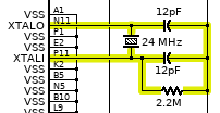
The 24 MHz crystal is required. As with all crystal oscillators, a solid ground plane should be routed on the PCB layer directly underneath the crystal. 2 capacitors and 1 resistor are required. See NXP's Hardware Development Guide for the MIMXRT1050/MIMXRT1060 Applications Processor, Rev.0, 08/2018 for details.The 32.768 kHz crystal is optional. If not used, the IMXRT will automatically use a low accuracy 32 kHz internal oscillator.
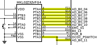
BGA Pinout Diagram
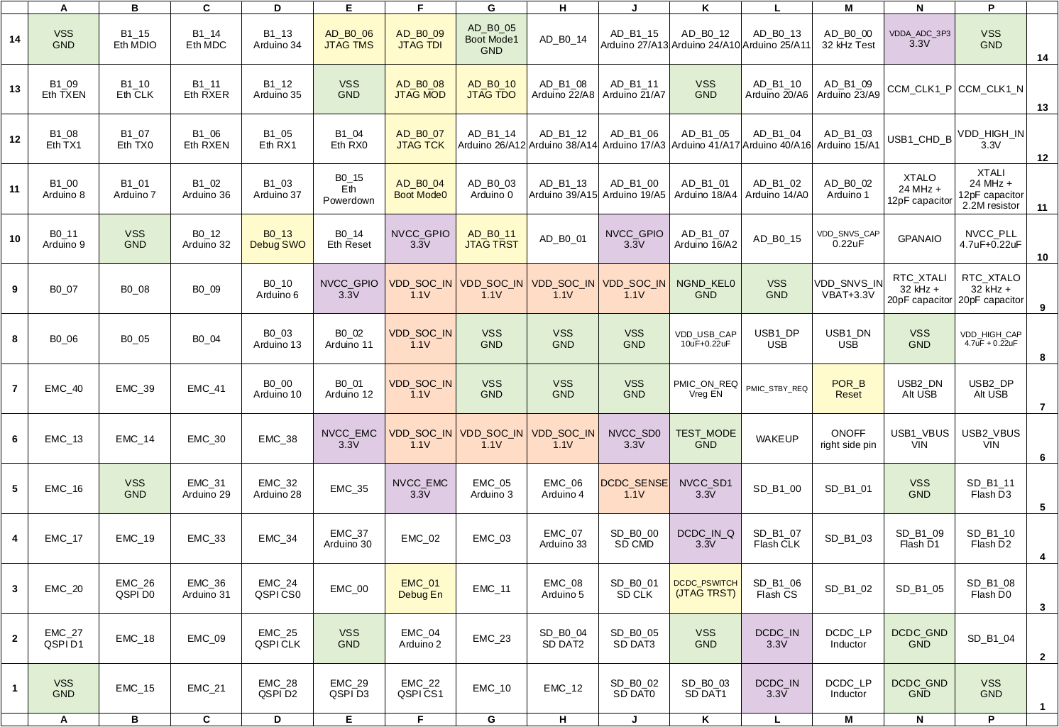
Printable PDF of this pinout diagram.
If you route I/O pins not normally used on any Teensy model, you will need to edit the Teensy core library to add support for those pins. You will also need to edit the Wire library if the 4th I2C port is used.
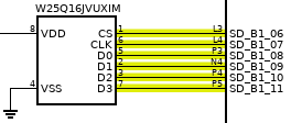
Avoid using SD_B1_05 (BGA pin N3) for I/O. Normally this pin should be left unconnected. The flash memory controller compensates for signal speed using this pin.
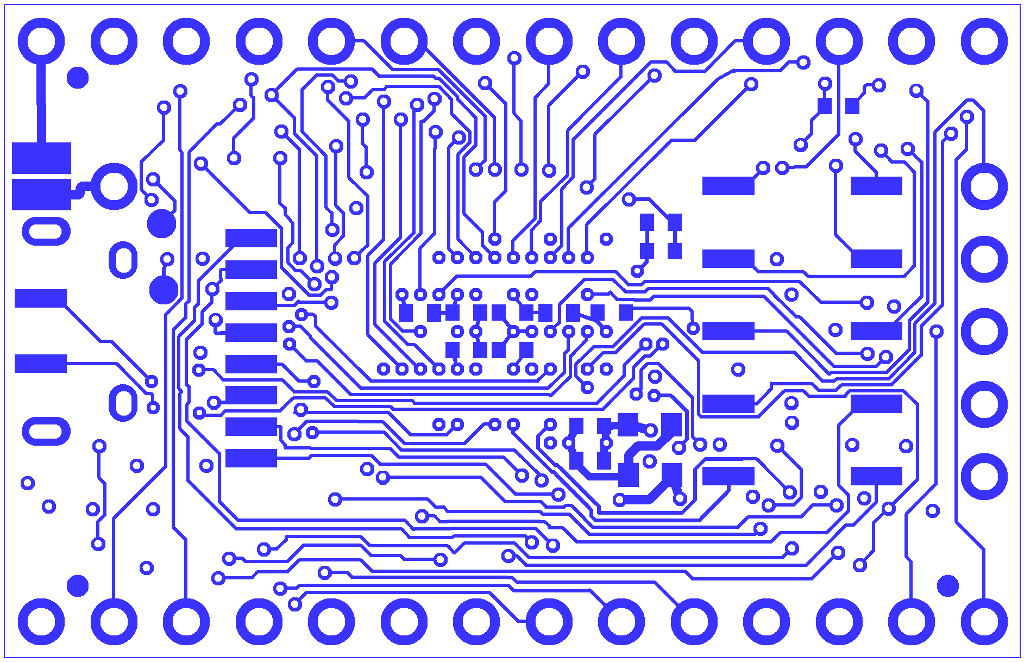
PCB Design and BGA Routing
Ball Grid Array (BGA) routing can feel daunting. Don't be intimidated. For inspiration, here is the PCB layout used for an early 4 layer Teensy 4.0 prototype.
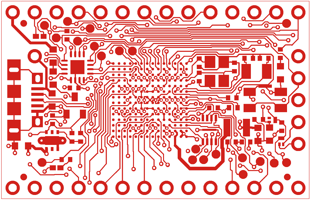

With the smaller 10x10mm BGA chip, where the pins are at 0.65mm pitch, signals and ground/power planes can not route between adjacent vias on other layers (unless using an expensive premium PCB process).
One BGA routing strategy is keep some rows free of vias. This approach allows only about half of all the pins to be used, which is plenty for the Teensy 4.0 design. The no-via rows allow power & ground to connect on the inner layers, and provide space for decoupling capacitors or signal routing on the bottom layer.
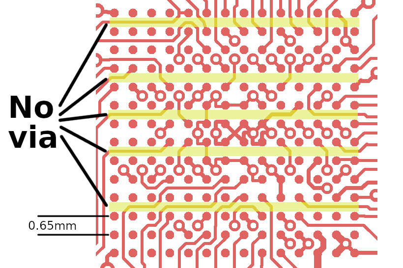
With the larger 12x12mm BGA chip, where the pins are at 0.8mm pitch, adjacent vias do allow a signal to route between them on other layers. For a design where more than 60% of the BGA pins must be routed, the larger 0.8mm pitch BGA chip allows use a standard PCB process.
Hardware Initialization
IMXRT fuses are initialized the first time the IMXRT1062 and MKL02 chip are used together. Bits 4 and 19 in the HW_OCOTP_CFG5 fuse word are set. Bit 4 allows booting from flash memory. Bit 19 configures IMXRT to communicate using JTAG.The HW_OCOTP_MAC0 and HW_OCOTP_MAC1 fuses are also set with unique 48 bit Ethernet Mac address. Only a single IMXRT1062 may be initialized.
The first time the Program button is pressed, the top 4K of flash memory is written with a known-good LED blink program. When the program button is pressed for 15 seconds, the rest of the flash chip is erased and this LED blink is copied to the beginning of the flash memory. Because this copy is created on the first non-15-second press, the 15 second press for restore only works if a short press for normal bootloader entry has been done at least once.
Code Security
Secure mode may be used with IC_MKL02Z32_T4_QFN16 sold starting November 1, 2021.
Secure mode provides these benefits.
- Program code stored in the flash memory chip is encrypted
- Only code encrypted by your key is allowed to run
- JTAG acccess is disabled
- Teensy Loader can securely update, even when run by untrused parties
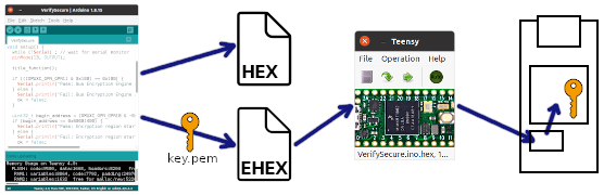
To use code security, in Arduino click Tools > Teensy 4 Security.
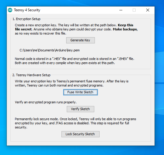
For each board, run the Fuse Write Sketch to store your key into permanent fuse memory. Optionally, run the Verify Sketch to confirm code really is running with encryption. Then run the Lock Security Sketch to permanently lock secure mode.
Full details can be found on the code security page.
IC_MKL02Z32_T4_QFN16 chips sold before August 12, 2021 do not support code security. Locking secure mode will make boards make boards with those chips forever unbootable! PJRC recommends disabling changes to boot configuration, so secure mode can not become locked.
Disabling Boot Configuration Changes
To permanently prevent changes to boot & security settings, run this program.
void setup() {
  /* Prevent changes to boot & security configuration */
  IMXRTfuseWrite(&HW_OCOTP_LOCK, 0x00400004);
}

void loop() {
}
If this program is run before secure mode is set, it will forever prevent locking secure mode. Changes to other fuses which might affect boot are also prohibited.
User Shared Projects
Jens Chr Brynildsen Kicad example project (GitHub) using USB-C connectors for device and host, extra pins routed to test pins.
Dogbone06 shared a
SDRAM-based circuit board
also with access to all FlexIO pins. Uses SDRAM_t4 library.
Troubleshooting & Diagnostic Blink Codes
If your custom board does not start up, first check the power supply. As described in the power supply startup sequence, the IMXRT internal voltage regulators must start first, then 3.3V power is turned on when PMIC_ON_REQ is driven high.When the MKL02 chip receives stable 3.3V power, it will activate an internal pullup resistor on the Program signal (pin 10, PTB2). It will also drive DCDC_PSWITCH (connected to pin 3, PTA3) initially low and then high after 3.3V has remained stable for several milliseconds. This behavior on pin 3, PTA3 and the weak pullup in pin 10, PTB2 can confirm if the MKL02 has started properly.
If DCDC_PSWITCH has been driven high, the buck converter should develop 1.15 volts at VDD_SOC_IN. The processor and nearly all digital logic inside the IMXRT depends on proper VDD_SOC_IN power.
Once running, the MKL02 will blink its red LED when error conditions are detected. The blinks appear at 0.6 seconds apart and if the error condition remains, the pattern repeats after a 2 second pause.
- 2 Blinks = NXP JTAG Not Responding
- No communication is working! The 2 likely causes for this problem
are improper power startup sequence, or a problem with any of these
connections between the MKL02 and IMXRT chip:
- 3 Blinks = Flash Chip Error, Missing or Incorrect ID
- The flash memory chip did not respond to the JEDEC ID query, or
it is an incompatible chip.
- 4 Blinks = ARM JTAG & SWD Not Responding (Needs Crystal)
- The NXP JTAG communication is working, but communication with ARM JTAG
or SWD fails. Usually this error means the 24 MHz crystal is not oscillating.
NXP's JTAG does not require the oscillator, but the ARM JTAG does. This error
also be caused by a bad connection between PTB5 to AD_B0_08, which is the signal
that selects which JTAG controller is accessible.
- 5 Blinks = Crystal Oscillator Is Unstable
- The OSC_XTALOK (bit 15) flag in XTALOSC24M_MISC0 reported the 24 MHz crystal oscillator is not stable.
- 6 Blinks = reserved
- This error is not used. It is reserved for future bootloader updates.
- 7 Blinks = ARM JTAG DAP Communication Error
- A communication error was detected, but after correctly detecting (4 blinks) and initializing the ARM JTAG DAP (9 blinks). Programs which crash or have unusual startup behavior can cause a temporary 7 blink error at startup. With a known-good program or blank flash chip, this error may indicate a severe signal quality problem or any of the signal wires shorted to other lines which are initially high impedance but become output after a program is running. But these types of hardware issues are unusual, because hardware trouble for 7 blinks requires first successfully passing tests which would cause 4 or 9 blinks. 7 blinks can also be shown if the processor reboots, either by software write to SCB_AIRCR or due to fault or other error handling, while communication is in progress. If you see 7 blinks, program the flash memory with a simple known-good code before investigating hardware trouble.
- 8 Blinks = Unknown IMXRT Chip
- The IMXRT chip responded, but with an unsupported JTAG ID. This error can happen if IMXRT AD_BO_08 is not connected to MKL02 PTB5, or it is shorted to GND. Software which mis-configures pins can also cause this error.
- 9 Blinks = ARM JTAG DAP Init Error
- The ARM JTAG DAP was detected (4 blinks) but could not be initialized. This error is rather unlikely by hardware! However, a software crash resulting in hard fault or CPU lockup (typically very early in startup) can result in this error.
- 10 Blinks = Serial Number Already Assigned
- A problem occurred with the serial number & ethernet mac address assignment.
- 11 Blinks = ARM SWD DAP Communication Error
- An communication error was detected in the initial IMXRT fuses setup.
- 12 Blinks = Unable To Halt IMXRT
- When attempting to enter bootloader mode, ARM JTAG communication is working (4, 7, 9 blinks) but the IMXRT M7 processor could not be halted to take control of the IMXRT chip.
- 13 Blinks = Unable To Access IMXRT Memory After CPU Halt
- When attempting to enter bootloader mode, the IMXRT M7 processor was successfully halted (5, 7, 9, 12 blinks) but then memory could not be accessed. This error is extremely unlikely.
- Alternating Red/Orange for 30 Seconds = Secure Access Failure
- Uploading to a chip locked into secure mode requires an initial loader utility step. If the loader utility passes initial authentication, but then experiences any error authenticating the bootloader process, the result is alternating blinks on red and orange LEDs for about 30 seconds. If this error happens on every upload attempt, you may need to create a new EHEX file with updated software.
Technical Support (Forum)
Please understand PJRC can not provide direct technical assistance with custom PCB design.Diagnosing problems with a brand new PCB design can be tough. If you are stuck, please consider posting a request for help on the public forum. You will need to show some or all of your custom PCB. Historically, many of the PCB designs using the Teensy 3.x bootloader chip were diagnosed on the forum. When those conversations yield valuable insight which may help others, we add links to those forum conversations from this page.
This Initial forum thread is where much of the bootloader chip development was discussed.