|
|
| ||
|
Shopping Cart
|
| Home | Products | Teensy | Blog | Forum |
|
You are here:
MP3 Player
|
|
|
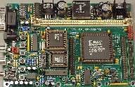
A Closer Look At The MP3 HardwareThese photos show the actual hardware that does the MP3 decoding and D/A conversion. Perhaps together with the hand written note these pictures may help you piece together enough info to build the circuit. This first photo shows the chip... it is taken at a slight angle, so that all the printing on the chips is readable. In particular, the printing on the MAS3507D is very light and hard to get a good picture showing it nicely.
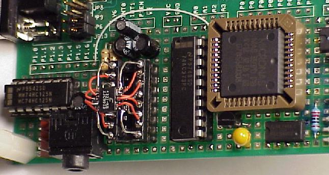
Well, at least the writing on the chips is somewhat readable. The Crystal CS4327 DAC only comes in the tiny SSOP package, which I soldered into a 16-pin DIP socket, as you can see here. It's a bit ugly, but it works ok for a prototype. The TO-92 package part near the bottom of the MAS3507D is a 2N3904 NPN transistor, which is connected common emitter (to ground), with the base driven from P1.7, and the collector (with 3 volt pullup) connected to the decoder's reset line. The decoder has an active low reset, but the 8051's port pins default to high when it reboots. The yellow cap near the transisor is a 22 uF tantalum capacitor, which decouples the 3 volt supply. The line that runs along the bottom edge of the board is ground. To the right of the crystal is the LM317 voltage regulator, which makes 3 volts using a 220 ohm and 330 ohm resistor. The 330 ohm resistor isn't visible in these pictures. The resistors and capacitors just above the DAC are pairs of 3 ohm (1.5 ohm for each one, four resistors total), and the caps are 100 uF, 6.3 volt. These parts low-pass filter the 5 volt supply, for the DAC. The smaller cap, near the PSEN and INT1 pads, is a 1 uF required by the DAC. Two capacitors are located near the output jack (one is mostly hidden by the wires supporting the DAC in mid-air). These caps couple the DAC's output and remove the 2.5 volt offset. I really should have used opamps with a low-pass filter, as suggested by the DAC's datasheet... I'll certainly do that in the next design, but as it is it sounds quite good into a pair of amplified speakers. This picture may be helpful if you should try to make some sense out of the two wiring photos below. Don't forget to mentally flip it as you compare to the photos of the bottom side. Point-To-Poing Wiring On The Board
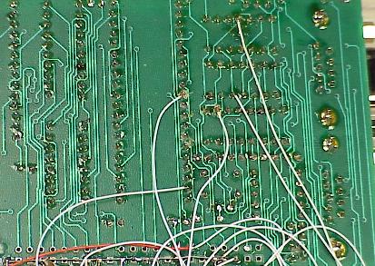
This photo shows the wiring to the MAS3507D, DAC, and the two logic chips that do the voltage level conversion and serial port switching. The MAS3507D requires a bunch of pullup resistors to configure it, and these are 0805 package surface mount, soldered on the bottom. The larger 1206 parts are 0.1 uF capactitors. At the lower left corner of this picture is a LM317 voltage regulator, which is used to produce the 3 volt power supply for the MP3 decoder chip. The crystal oscillator and 74AC373 also run on 3 volts. The 74AC373 isn't used as a latch... the clock (pin 11) is tied high, so it basically acts as 8 non-inverting buffers. Pins 12 and 13 are used to buffer the MAS3507D's data demand signal, which may not be necessary, but I didn't want the 8051's internal pullup transistor on P1.6 to source current into the (expensive) decoder chip. A small resistor prevents the '373 from taking a lot of current into its protection diode when the 8051 makes a low-to-high transition and turns on it's strong pullup transistor for a short time. The only other two buffers used from the '373 are on pins 2 though 5, for the 8051's serial data and clock signals. Again, a couple resistors on pins 3 and 4 help protect the 373 chip. Perhaps the 373 isn't even necessary at all, but since I only ordered two MAS3507D chips, and they were expensive, I decided to play it safe, and I had the 373 chip laying around. The 74HC125 chip has only one of its 3-state buffers used, on pins 11, 12, and 13, and it's used to enable reception for the 8051 when the normal serial port is needed (Paulmon2) and to disconnect the receive signal, since the 8051's RXD pin must become at output pin in mode 0, and it doesn't take kindly to being driven by the NAND gate (pin 11 of U7).
|