skip navigational linksPJRC
Shopping Cart Download Website
Home Products Teensy Blog Forum
You are here: 8051 Tools Development Board Troubleshooting Memory

PJRC Store
8051 Board, $79
LCD 128x64 Pixel, $29
LCD 16x2 Char, $14
Serial Cable, $5
9 Volt Power, $6
More Components...
8051 Tools
Main Page
Software
PAULMON Monitor
Development Board
Code Library
89C2051 Programmer
Other Resources

Memory Testing

This page is primarily intended for troubleshooting boards built from the unassembled kit. All boards assembled at PJRC have their memory thoughly tested before they are shipped. This information may also be useful for anyone who built this design using wire wrap, point-to-point soldering, or breadboard construction; if a pre-programmed 87C52 chip was used, and the power, reset, crystal and serial port are functioning to allow access to the PAULMON2 memory editor.

No technical support (other than this page) is available from PJRC for custom designed circuit boards or hand wired construction, even if it is closely based on this site's free schematics and other technical information. Assistance is available for problematic boards built from the unassembled kit sold by PJRC.

There is no simple, easy test to determine which signals are not connected properly. The process involves using the memory editor to read, write and observe changes in the memory, looking for incorrect behavior. Once you see the memory respond erronously, with careful thought and analysis, you may be able to deduce what signals are likely to cause the behavior you observe in the memory editor.

This page reverses this process. Known errors are created, and then the resulting memory behavior is explained. If you are lucky (but not lucky enough to get all signals connected properly on the first try), your board's behavior may closely match one of these scenarios. If not, this page may at least illustrate the basic principle and give you some initial experience to get you started on the path to understanding what is wrong.

But first, before staring at screen after screen of memory editor display, there are some simple tests.

Checking Each Memory Type

Before digging into details with the memory editor, you can simply try to download files into each memory type. This should first be tried with all chips on the board, and alternately with only the target chip installed. This can give you a very quick check if a problem is with only one type of memory, or all types, and if there is some interaction (eg, the damaged RAM chip may interfere with using the flash chip which is not damaged).

Download To RAM

This code downloads to the RAM chip at 0x2000.

blink_ram.hex

A correct download of this file should show this summary:

Summary:
 14  lines received
 198  bytes received
 198  bytes written
No errors detected

Download To Flash ROM

This code downloads to the Flash ROM chip at 0xF000.

blink_flash.hex

A correct download of this file should show this summary:

Summary:
 14  lines received
 198  bytes received
 198  bytes written
No errors detected

Download To 82C55/LEDs Directly

This file is a sequence of 1649 writes directly to the 82C55 chip which controls the 8 LEDs. The first write configures the chip, and the remaining 1648 writes disply a pattern where one LED is on at a time, starting with the one closest to the prototype area.

blink_82c55.hex

A correct download of this file should show this summary, with 1 error:

Summary:
 1650  lines received
 1649  bytes received
 1648  bytes written
Errors:
 1  bytes unable to write

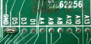
The "unable to write" error is correct behavior. The 82C55 chip configuration register is write-only, so when PAULMON2 attempts to verify by reading back from that location, it does not get the same byte that was written.

At 115200 baud, this download takes approximately 2 seconds. The LEDs display one on in an animated sequence from bottom to top. If you see this animation during the download, the 82c55 chip is receiving the data properly.

Memory Editor Techniques

The PAULMON2 memory editor can help you to "see" how your memory chips are responding. This approach can provide strong indication of what is wrong with your board. However, it requires understanding how the memory editor works (easy), and deducing what may be wrong with the hardware from observing the incorrect behavior (not as easy).

The most important point about the memory editor is that it attempts to always show you the memory as it is read over the 8051's external bus. When you modify the conents of any location, the memory editor writes you new byte, then reads the memory and shows the value it read on the screen. The byte you typed it not shown... the actual value read back is what you see on the screen.

However, when entering 8 bit hexidecimal values, your first keystroak is held in a register and the screen is updated with that value. When you make the second keystroak, your 8 bit number is written to memory. Then the memory is read from that same location and the value returned from the chip is shown on the screen. Do not confuse this first keystroak with working memory. It is being held in a register and the actual memory interaction takes place on the second keystroak.

Likewise, only the byte you have just changed is refreshed on the screen. All others remain the same on the screen to avoid excessive (and slow) serial communication to update the full display. When testing memory, you will frequently type CTRL-L to cause the entire 256 byte display to refresh. Many types of problems with address lines are only observable by refreshing the full screen.

Concentrate on the RAM first. The memory editor performs a sequence of write operations to write into the flash rom. Most wiring errors cause the flash chip to be utterly unwritable. If your board has a wiring or connectivity error, editing the RAM is your best chance to diagnose it.

Case 1: Data Line Stuck At Zero

In this first example, the D5 line is stuck at zero. This is a relatively simple problem to detect. If your board has a solder bridge like the one shown in Figure 1, you should have no problem discovering the nature of the error. Likewise, an open circuit (or poor solder connection) will often give similar behavior, stuck at zero or stuck at one.

photo: pins shorted
Figure 1: Signal D5 Shorted To Ground

When the memory editor is first entered, nothing initially appears to be wrong. Perhaps some people could notice that none of these 256 bytes has its D5 bit set?

Because nearly all problems are observed by noticing the difference between an expected change in the display and the actual change that takes place, this page includes the initial display in each of these examples.

CODE        8051 External Memory Editor, Paul Stoffregen, 1996
ADDR: +0 +1 +2 +3 +4 +5 +6 +7 +8 +9 +A +B +C +D +E +F   ASCII EQUIVILANT
------------------------------------------------------------------------
2000: 00 09 02 89 8B 8D 02 02 01 15 04 94 16 D7 40 42                W@B
2010: 01 0A 06 CF 05 9E 00 1F 00 C0 C6 18 48 5E 14 46      O     @F H^ F
2020: 00 09 02 89 8B 8D 02 02 01 15 04 94 16 D7 40 42                W@B
2030: 01 0A 06 CF 05 9E 00 1F 00 C0 C6 18 48 5E 14 46      O     @F H^ F
2040: 51 00 01 41 19 D4 02 D6 18 9C CD 89 00 1C 01 5C   Q  A T V  M    \
2050: 00 04 00 97 08 13 00 D8 10 10 85 D5 40 16 00 0E          X   U@   
2060: 51 00 01 41 19 D4 02 D6 18 9C CD 89 00 1C 01 5C   Q  A T V  M    \
2070: 00 04 00 97 08 13 00 D8 10 10 85 D5 40 16 00 0E          X   U@   
2080: 00 46 00 43 90 0C 84 DE 0C C6 00 57 53 08 08 DA    F C   ^ F WS  Z
2090: 00 C6 04 08 02 4C 00 84 00 D7 0A 13 0C 4C 04 59    F   L   W   L Y
20A0: 00 46 00 43 90 0C 84 DE 0C C6 00 57 53 08 08 DA    F C   ^ F WS  Z
20B0: 00 C6 04 08 02 4C 00 84 00 D7 0A 13 0C 4C 04 59    F   L   W   L Y
20C0: 00 42 02 02 81 C4 00 19 00 C5 81 D2 10 D1 00 05    B   D   E R Q  
20D0: 00 86 C2 C8 4A 15 00 5E 49 90 01 59 13 10 98 D3     BHJ  ^I  Y   S
20E0: 00 42 02 02 81 C4 00 19 00 C5 81 D2 10 D1 00 05    B   D   E R Q  
20F0: 00 86 C2 C8 4A 15 00 5E 49 90 01 59 13 10 98 D3     BHJ  ^I  Y   S
------------------------------------------------------------------------
^E-Edit  ^G=Goto  ^C=Code  ^D=Data  ^L=Redraw  ^Q=Quit

Usually, the first step is to press CTRL-E to enable editing, and then type several bytes to begin testing the memory. On the examples for this page, the pattern "0102040810204080" was typed. This enters 8 bytes where each has one bit set. Entering 00, FF, and 8 more with all but one bit set can also be helpful.

In this case, the error is easy to see:

CODE        8051 External Memory Editor, Paul Stoffregen, 1996
ADDR: +0 +1 +2 +3 +4 +5 +6 +7 +8 +9 +A +B +C +D +E +F   ASCII EQUIVILANT
------------------------------------------------------------------------
2000: 01 02 04 08 10 00 40 80 01 15 04 94 16 D7 40 42         @      W@B
2010: 01 0A 06 CF 05 9E 00 1F 00 C0 C6 18 48 5E 14 46      O     @F H^ F
2020: 01 02 04 08 10 00 40 80 01 02 04 08 10 00 40 80         @       @ 
2030: 01 0A 06 CF 05 9E 00 1F 00 C0 C6 18 48 5E 14 46      O     @F H^ F
2040: 51 00 01 41 19 D4 02 D6 18 9C CD 89 00 1C 01 5C   Q  A T V  M    \
2050: 00 04 00 97 08 13 00 D8 10 10 85 D5 40 16 00 0E          X   U@   
2060: 51 00 01 41 19 D4 02 D6 18 9C CD 89 00 1C 01 5C   Q  A T V  M    \
2070: 00 04 00 97 08 13 00 D8 10 10 85 D5 40 16 00 0E          X   U@   
2080: 00 46 00 43 90 0C 84 DE 0C C6 00 57 53 08 08 DA    F C   ^ F WS  Z
2090: 00 C6 04 08 02 4C 00 84 00 D7 0A 13 0C 4C 04 59    F   L   W   L Y
20A0: 00 46 00 43 90 0C 84 DE 0C C6 00 57 53 08 08 DA    F C   ^ F WS  Z
20B0: 00 C6 04 08 02 4C 00 84 00 D7 0A 13 0C 4C 04 59    F   L   W   L Y
20C0: 00 42 02 02 81 C4 00 19 00 C5 81 D2 10 D1 00 05    B   D   E R Q  
20D0: 00 86 C2 C8 4A 15 00 5E 49 90 01 59 13 10 98 D3     BHJ  ^I  Y   S
20E0: 00 42 02 02 81 C4 00 19 00 C5 81 D2 10 D1 00 05    B   D   E R Q  
20F0: 00 86 C2 C8 4A 15 00 5E 49 90 01 59 13 10 98 D3     BHJ  ^I  Y   S
------------------------------------------------------------------------
^A=ASCII  ^X=Hex  ^F=Fill  ^G=Goto  ^C=Code  ^D=Data  ^L=Redraw  ^Q=Quit

The byte at position 2005 is 00, when it should have been 20. Looking at these images does not have the visual impact that you get the instant your finger strikes that '0' key, and rather than "20" appearing, you see "00". In this case, it is very quick and easy to see the error and deduce that the D5 bit is not working properly.

Note: all data line problems are also effectively address line problems because of the multiplexed bus design. In this section, we have ignored this effect for the sake of simplicity. See case #3.

Case 2: Data Lines Shorted Together

This second example is very similar to the first one, but two data lines are shorted together.

photo: pins shorted
Figure 2: Signals D6 and D7 Shorted Together

Again, when viewing the initial screen, it's not immediately obvious that all these bytes have their D6 and D7 bits the same.

CODE        8051 External Memory Editor, Paul Stoffregen, 1996
ADDR: +0 +1 +2 +3 +4 +5 +6 +7 +8 +9 +A +B +C +D +E +F   ASCII EQUIVILANT
------------------------------------------------------------------------
2000: 28 D9 02 C9 CB CD 02 02 01 15 05 F4 16 F7 C0 E2   (Y IKM     t w@b
2010: 01 0A 06 CF 05 DE 00 1F 04 E0 C6 38 C0 DE 34 C6      O ^   `F8@^4F
2020: F1 EB FB 14 FD DC F5 CB D6 17 CE F0 F7 0F FF DB   qk{ }\uKV Npw  [
2030: FD EE DB CC F7 E0 FB 0F FF CE 3B D7 F7 3C FF C9   }n[Lw`{  N;Ww< I
2040: 28 D9 02 C9 CB CD 02 02 01 15 05 F4 16 F7 C0 E2   (Y IKM     t w@b
2050: 01 0A 06 CF 05 DE 00 1F 04 E0 C6 38 C0 DE 34 C6      O ^   `F8@^4F
2060: F1 EB FB 14 FD DC F5 CB D6 17 CE F0 F7 0F FF DB   qk{ }\uKV Npw  [
2070: FD EE DB CC F7 E0 FB 0F FF CE 3B D7 F7 3C FF C9   }n[Lw`{  N;Ww< I
2080: 28 D9 02 C9 CB CD 02 02 01 15 05 F4 16 F7 C0 E2   (Y IKM     t w@b
2090: 01 0A 06 CF 05 DE 00 1F 04 E0 C6 38 C0 DE 34 C6      O ^   `F8@^4F
20A0: F1 EB FB 14 FD DC F5 CB D6 17 CE F0 F7 0F FF DB   qk{ }\uKV Npw  [
20B0: FD EE DB CC F7 E0 FB 0F FF CE 3B D7 F7 3C FF C9   }n[Lw`{  N;Ww< I
20C0: 20 E2 22 02 E1 C4 00 19 00 C5 C1 F6 14 D1 02 25    b" aD   EAv Q %
20D0: 00 C6 E2 E8 EA 15 00 DE C9 D0 01 F9 13 30 D8 D3    Fbhj  ^IP y 0XS
20E0: F6 D0 1A 13 F7 E6 FF 03 DB DA FE D5 C5 D7 FF D3   vP  wf  [Z~UEW S
20F0: FF D4 ED C1 3E F8 FE ED 2F DA F3 F5 D9 DD FF E2    TmA>x~m/ZsuY] b
------------------------------------------------------------------------
^E-Edit  ^G=Goto  ^C=Code  ^D=Data  ^L=Redraw  ^Q=Quit

As before, once you start editing, the problem turns up quickly.

Here, CTRL-E was pressed to allow editing, and "0102040810204080" was typed to enter 8 test bytes.

CODE        8051 External Memory Editor, Paul Stoffregen, 1996
ADDR: +0 +1 +2 +3 +4 +5 +6 +7 +8 +9 +A +B +C +D +E +F   ASCII EQUIVILANT
------------------------------------------------------------------------
2000: 01 02 04 08 10 20 C0 C0 01 15 05 F4 16 F7 C0 E2         @@   t w@b
2010: 01 0A 06 CF 05 DE 00 1F 04 E0 C6 38 C0 DE 34 C6      O ^   `F8@^4F
2020: F1 EB FB 14 FD DC F5 CB D6 17 CE F0 F7 0F FF DB   qk{ }\uKV Npw  [
2030: FD EE DB CC F7 E0 FB 0F FF CE 3B D7 F7 3C FF C9   }n[Lw`{  N;Ww< I
2040: 28 D9 02 C9 CB CD 02 02 01 15 05 F4 16 F7 C0 E2   (Y IKM     t w@b
2050: 01 0A 06 CF 05 DE 00 1F 04 E0 C6 38 C0 DE 34 C6      O ^   `F8@^4F
2060: F1 EB FB 14 FD DC F5 CB D6 17 CE F0 F7 0F FF DB   qk{ }\uKV Npw  [
2070: FD EE DB CC F7 E0 FB 0F FF CE 3B D7 F7 3C FF C9   }n[Lw`{  N;Ww< I
2080: 28 D9 02 C9 CB CD 02 02 01 15 05 F4 16 F7 C0 E2   (Y IKM     t w@b
2090: 01 0A 06 CF 05 DE 00 1F 04 E0 C6 38 C0 DE 34 C6      O ^   `F8@^4F
20A0: F1 EB FB 14 FD DC F5 CB D6 17 CE F0 F7 0F FF DB   qk{ }\uKV Npw  [
20B0: FD EE DB CC F7 E0 FB 0F FF CE 3B D7 F7 3C FF C9   }n[Lw`{  N;Ww< I
20C0: 20 E2 22 02 E1 C4 00 19 00 C5 C1 F6 14 D1 02 25    b" aD   EAv Q %
20D0: 00 C6 E2 E8 EA 15 00 DE C9 D0 01 F9 13 30 D8 D3    Fbhj  ^IP y 0XS
20E0: F6 D0 1A 13 F7 E6 FF 03 DB DA FE D5 C5 D7 FF D3   vP  wf  [Z~UEW S
20F0: FF D4 ED C1 3E F8 FE ED 2F DA F3 F5 D9 DD FF E2    TmA>x~m/ZsuY] b
------------------------------------------------------------------------
^A=ASCII  ^X=Hex  ^F=Fill  ^G=Goto  ^C=Code  ^D=Data  ^L=Redraw  ^Q=Quit

At location 2006, the incorrect "C0" is seen rather than "40", and the same occurs at 2007 rather than "80". In each of these cases, one line is driving low and the other high. By chance, both bits ended up being written as 1s to the memory, and then read back as 1s.

The bits read back could be either both zero or both one. In this case, they were both one. If they had happened to be both zero, you might at first believe both D6 and D7 were stuck at zero. Using more tests with 00, FF, FE, FD, FB, F7, EF, DF, BF and 7F would quickly reveal that those two bits were not stuck at a particular value. Usually, the 8 simple cases with only 1 bit set are enough to quickly discover a problem, but if the error is not clear, trying 00, FF and the 8 bytes with only all but one bit set to 1 help provide more information.

Note: all data line problems are also effectively address line problems because of the multiplexed bus design. In this section, we have ignored this effect for the sake of simplicity. See case #3.

Case 3: Lower Address Line Stuck At Zero

Now, let's look at the more difficult case where an address line is not connected properly. This can also easily be detected using the memory editor, but the technique is different.

photo: pins shorted
Figure 3: Signal A3 Shorted To Ground

As usual, the initial memory editor screen does not make the problem obvious, though someone very observant might notice that groups of bytes are duplicated. Rarely is your time well spent staring at the initial display, because the problem will become very obvious as you interact with the memory.

CODE        8051 External Memory Editor, Paul Stoffregen, 1996
ADDR: +0 +1 +2 +3 +4 +5 +6 +7 +8 +9 +A +B +C +D +E +F   ASCII EQUIVILANT
------------------------------------------------------------------------
2000: 20 19 02 89 8B 8D 02 02 20 19 02 89 8B 8D 02 02                   
2010: 01 0A 06 CF 05 9E 00 1F 01 0A 06 CF 05 9E 00 1F      O       O    
2020: F3 6B FB 14 FD 9C F5 CB F3 6B FB 14 FD 9C F5 CB   sk{ } uKsk{ } uK
2030: FD EE DB C8 B7 A0 FB 0F FD EE DB C8 B7 A0 FB 0F   }n[H7 { }n[H7 { 
2040: F1 04 01 41 99 D4 02 96 F1 04 01 41 99 D4 02 96   q  A T  q  A T  
2050: 00 24 00 B7 28 33 02 D8 00 24 00 B7 28 33 02 D8    $ 7(3 X $ 7(3 X
2060: FD 7A FF 32 C6 80 BD 45 FD 7A FF 32 C6 80 BD 45   }z 2F =E}z 2F =E
2070: E7 17 DF C9 1F 2C FE 0F E7 17 DF C9 1F 2C FE 0F   g _I ,~ g _I ,~ 
2080: 00 67 00 43 B0 2C A4 DE 00 67 00 43 B0 2C A4 DE    g C0,$^ g C0,$^
2090: 08 C6 04 28 02 4C 00 84 08 C6 04 28 02 4C 00 84    F ( L   F ( L  
20A0: 5B 0E F4 4E EF 2A C6 9E 5B 0E F4 4E EF 2A C6 9E   [ tNo*F [ tNo*F 
20B0: DD 55 B9 ED DA D5 DF E8 DD 55 B9 ED DA D5 DF E8   ]U9mZU_h]U9mZU_h
20C0: 00 E2 02 00 A1 C4 00 19 00 E2 02 00 A1 C4 00 19    b  !D   b  !D  
20D0: 00 A6 E2 C8 6A 15 00 5E 00 A6 E2 C8 6A 15 00 5E    &bHj  ^ &bHj  ^
20E0: F6 50 1A 13 F7 E6 FF 03 F6 50 1A 13 F7 E6 FF 03   vP  wf  vP  wf  
20F0: FF 54 CD C1 3E 78 FE AF FF 54 CD C1 3E 78 FE AF    TMA>x~/ TMA>x~/
------------------------------------------------------------------------
^E-Edit  ^G=Goto  ^C=Code  ^D=Data  ^L=Redraw  ^Q=Quit

As before, CTRL-E is pressed to enable editing, and the "0102040810204080" is typed to enter the basic 8 byte test pattern that worked so well in the previous two examples.

CODE        8051 External Memory Editor, Paul Stoffregen, 1996
ADDR: +0 +1 +2 +3 +4 +5 +6 +7 +8 +9 +A +B +C +D +E +F   ASCII EQUIVILANT
------------------------------------------------------------------------
2000: 01 02 04 08 10 20 40 80 01 19 02 89 8B 8D 02 02         @         
2010: 01 0A 06 CF 05 9E 00 1F 01 0A 06 CF 05 9E 00 1F      O       O    
2020: F3 6B FB 14 FD 9C F5 CB F3 6B FB 14 FD 9C F5 CB   sk{ } uKsk{ } uK
2030: FD EE DB C8 B7 A0 FB 0F FD EE DB C8 B7 A0 FB 0F   }n[H7 { }n[H7 { 
2040: F1 04 01 41 99 D4 02 96 F1 04 01 41 99 D4 02 96   q  A T  q  A T  
2050: 00 24 00 B7 28 33 02 D8 00 24 00 B7 28 33 02 D8    $ 7(3 X $ 7(3 X
2060: FD 7A FF 32 C6 80 BD 45 FD 7A FF 32 C6 80 BD 45   }z 2F =E}z 2F =E
2070: E7 17 DF C9 1F 2C FE 0F E7 17 DF C9 1F 2C FE 0F   g _I ,~ g _I ,~ 
2080: 00 67 00 43 B0 2C A4 DE 00 67 00 43 B0 2C A4 DE    g C0,$^ g C0,$^
2090: 08 C6 04 28 02 4C 00 84 08 C6 04 28 02 4C 00 84    F ( L   F ( L  
20A0: 5B 0E F4 4E EF 2A C6 9E 5B 0E F4 4E EF 2A C6 9E   [ tNo*F [ tNo*F 
20B0: DD 55 B9 ED DA D5 DF E8 DD 55 B9 ED DA D5 DF E8   ]U9mZU_h]U9mZU_h
20C0: 00 E2 02 00 A1 C4 00 19 00 E2 02 00 A1 C4 00 19    b  !D   b  !D  
20D0: 00 A6 E2 C8 6A 15 00 5E 00 A6 E2 C8 6A 15 00 5E    &bHj  ^ &bHj  ^
20E0: F6 50 1A 13 F7 E6 FF 03 F6 50 1A 13 F7 E6 FF 03   vP  wf  vP  wf  
20F0: FF 54 CD C1 3E 78 FE AF FF 54 CD C1 3E 78 FE AF    TMA>x~/ TMA>x~/
------------------------------------------------------------------------
^A=ASCII  ^X=Hex  ^F=Fill  ^G=Goto  ^C=Code  ^D=Data  ^L=Redraw  ^Q=Quit

After entering the 8 bytes, the memory appears to be working perfectly. This is because each on-screen byte is the result of reading back only that byte after having written it. The other 255 bytes remain the same on-screen, because they are being held in the buffer of your PC's terminal emulator. Those other 255 bytes are old information stored on your PC, not the current state of the circuit board's observable memory.

The next step is to press CTRL-L. For simplicity, this was not mentioned in the previous 2 examples. However, you should ALWAYS try pressing CTRL-L. Normally, nothing should change. When bytes change unexpectedly, you immediately know something is wrong, and that something is typically an error on the lower 8 address lines.

CODE        8051 External Memory Editor, Paul Stoffregen, 1996
ADDR: +0 +1 +2 +3 +4 +5 +6 +7 +8 +9 +A +B +C +D +E +F   ASCII EQUIVILANT
------------------------------------------------------------------------
2000: 01 02 04 08 10 20 40 80 01 02 04 08 10 20 40 80         @       @ 
2010: 01 0A 06 CF 05 9E 00 1F 01 0A 06 CF 05 9E 00 1F      O       O    
2020: F3 6B FB 14 FD 9C F5 CB F3 6B FB 14 FD 9C F5 CB   sk{ } uKsk{ } uK
2030: FD EE DB C8 B7 A0 FB 0F FD EE DB C8 B7 A0 FB 0F   }n[H7 { }n[H7 { 
2040: F1 04 01 41 99 D4 02 96 F1 04 01 41 99 D4 02 96   q  A T  q  A T  
2050: 00 24 00 B7 28 33 02 D8 00 24 00 B7 28 33 02 D8    $ 7(3 X $ 7(3 X
2060: FD 7A FF 32 C6 80 BD 45 FD 7A FF 32 C6 80 BD 45   }z 2F =E}z 2F =E
2070: E7 17 DF C9 1F 2C FE 0F E7 17 DF C9 1F 2C FE 0F   g _I ,~ g _I ,~ 
2080: 00 67 00 43 B0 2C A4 DE 00 67 00 43 B0 2C A4 DE    g C0,$^ g C0,$^
2090: 08 C6 04 28 02 4C 00 84 08 C6 04 28 02 4C 00 84    F ( L   F ( L  
20A0: 5B 0E F4 4E EF 2A C6 9E 5B 0E F4 4E EF 2A C6 9E   [ tNo*F [ tNo*F 
20B0: DD 55 B9 ED DA D5 DF E8 DD 55 B9 ED DA D5 DF E8   ]U9mZU_h]U9mZU_h
20C0: 00 E2 02 00 A1 C4 00 19 00 E2 02 00 A1 C4 00 19    b  !D   b  !D  
20D0: 00 A6 E2 C8 6A 15 00 5E 00 A6 E2 C8 6A 15 00 5E    &bHj  ^ &bHj  ^
20E0: F6 50 1A 13 F7 E6 FF 03 F6 50 1A 13 F7 E6 FF 03   vP  wf  vP  wf  
20F0: FF 54 CD C1 3E 78 FE AF FF 54 CD C1 3E 78 FE AF    TMA>x~/ TMA>x~/
------------------------------------------------------------------------
^A=ASCII  ^X=Hex  ^F=Fill  ^G=Goto  ^C=Code  ^D=Data  ^L=Redraw  ^Q=Quit

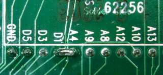
In this example, the bytes from 2008 to 200F unexpectedly change when CTRL-L is pressed. We know that this is because the A3 line is stuck at zero, as shown in figure 3.

Deducing which address lines are bad can be tricky, especially when the error is a more difficult open-circuit that can fail as a 1 or 0 (and may change between attempts, or may be different depending on what data was previously transfered). Luckily, there are only 8 address lines to check when you see bytes mysteriously change after a CTRL-L.

Warning: many multimeters output a large test current when used on their lower resistance measurement ranges, or their continuity (beeper) mode. If this test current flows through the static discharge protection diodes on a chip, that pin or the entire chip can be damaged. Check your multimeter's current level, and to be cautious, disable auto-ranging to force it to only output a safe current (less than 20 µA) for probing connectivity on the board while chips are installed in their sockets.

Case 4: Upper Address Line Stuck At Zero

In this example, A11 is shorted to ground. Sorry, no photo this time.

Because the memory editor shows only 256 bytes at a time, it really isn't very useful for dianosing this type of problem. All the steps shown above will indicate that the memory is functioning properly.

Fortunately, this type of problem is easy to see by just download blink_ram.hex. Everything appears normal at first:

Download completed

Summary:
 14  lines received
 198  bytes received
 198  bytes written
No errors detected

However, if you press "M", it will appear there are two copies in memory:

PAULMON2 Loc:2000 > List programs

Program Name                     Location      Type
  List                             1000      External command
  Single-Step                      1400      External command
  Memory Editor (VT100)            1800      External command
  Blink LEDs                       2000      Program
  Blink LEDs                       2800      Program

The program can be run, and it prints correct output to the serial port. But the LEDs do not work, because attempts to write to the 82C55 chip at 0xF100 requires A11 to be one. Had the same error been on A10, the LEDs would work, but a second copy of the program would have appeared at 2400. A larger program would have overwritten itself at not been able to work properly.

Connection problems on the upper address lines can be tricky, because many things will be able to work, or work partially with the good lower address lines and data bus. The memory editor only shows 256 bytes on the screen at a time, and everything will appear to work unless you very carefully compare different screens to each other (not easy). Duplicate copies of the program appearing in memory is the best indication of a problem on the upper address pins.

Case 5: Address Line Shorted To Data Line

So far, the previous 4 cases covered data line problems, where the error is quickly recognizable, or address line problems, where any single byte works but other bytes mysteriously change. If you are very unluckly, you could have both problems at the same time!

photo: pins shorted
Figure 4: Signal D1 Shorted To Signal A4

In this case, a data line is shorted to an address line. As a result, we'll likely see both types of behavior.

Unlike the previous cases, this initial memory editor screen "looks funny". There are several unlikely, visually recognizable patterns. But as before, guessing based on the initial display is difficult and observing behavior during editing is easy.

CODE        8051 External Memory Editor, Paul Stoffregen, 1996
ADDR: +0 +1 +2 +3 +4 +5 +6 +7 +8 +9 +A +B +C +D +E +F   ASCII EQUIVILANT
------------------------------------------------------------------------
2000: 20 A9 20 A9 8B 8D 8B 8D 01 15 01 15 96 5E 96 5E    ) )         ^ ^
2010: 06 CF 06 CF 02 1F 02 1F C6 3A C6 3A 36 46 36 46    O O    F:F:6F6F
2020: F3 EE F3 EE ED 9C ED 9C FF CE FF CE F7 0F F7 0F   snsnm m  N Nw w 
2030: DB CE DB CE FB 0F FB 0F 3B D7 3B D7 EF 83 EF 83   [N[N{ { ;W;Wo o 
2040: F1 00 F1 00 99 D4 99 D4 38 98 38 98 00 34 00 34   q q  T T8 8  4 4
2050: 02 B7 02 B7 02 DA 02 DA 87 F7 87 F7 02 2E 02 2E    7 7 Z Z w w . .
2060: FD 17 FD 17 1F 80 1F 80 F7 FA F7 FA D7 8E D7 8E   } }     wzwzW W 
2070: DF DB DF DB FE 0F FE 0F EB 82 EB 82 22 66 22 66   _[_[~ ~ k k "f"f
2080: 00 C6 00 C6 B0 6C B0 6C 2C F7 2C F7 73 28 73 28    F F0l0l,w,ws(s(
2090: 06 2A 06 2A 02 86 02 86 0A 33 0A 33 26 7B 26 7B    * *     3 3&{&{
20A0: 5B 0E 5B 0E DA D5 DA D5 FF 96 FF 96 FE FB FE FB   [ [ ZUZU    ~{~{
20B0: BB EF BB EF DB EA DB EA 6B EB 6B EB B7 E6 B7 E6   ;o;o[j[jkkkk7f7f
20C0: 00 A6 00 A6 A1 C4 A1 C4 00 C5 00 C5 14 D1 14 D1    & &!D!D E E Q Q
20D0: E2 CA E2 CA 02 5E 02 5E 03 7B 03 7B 9A D3 9A D3   bJbJ ^ ^ { { S S
20E0: FF 54 FF 54 3E EE 3E E6 2F DA 2F DA C5 D7 C5 D7    T T>n>f/Z/ZEWEW
20F0: EF C3 EF C3 FE AF FE AF B3 F7 B3 F7 FF EA FF EA   oCoC~/~/3w3w j j
------------------------------------------------------------------------
^E-Edit  ^G=Goto  ^C=Code  ^D=Data  ^L=Redraw  ^Q=Quit

As usual, CTRL-E was pressed, and then "0102040810204080" was typed to do the simple 8 byte test.

CODE        8051 External Memory Editor, Paul Stoffregen, 1996
ADDR: +0 +1 +2 +3 +4 +5 +6 +7 +8 +9 +A +B +C +D +E +F   ASCII EQUIVILANT
------------------------------------------------------------------------
2000: 01 00 04 08 10 20 40 80 01 15 01 15 96 5E 96 5E         @      ^ ^
2010: 06 CF 06 CF 02 1F 02 1F C6 3A C6 3A 36 46 36 46    O O    F:F:6F6F
2020: F3 EE F3 EE ED 9C ED 9C FF CE FF CE F7 0F F7 0F   snsnm m  N Nw w 
2030: DB CE DB CE FB 0F FB 0F 3B D7 3B D7 EF 83 EF 83   [N[N{ { ;W;Wo o 
2040: F1 00 F1 00 99 D4 99 D4 38 98 38 98 00 34 00 34   q q  T T8 8  4 4
2050: 02 B7 02 B7 02 DA 02 DA 87 F7 87 F7 02 2E 02 2E    7 7 Z Z w w . .
2060: FD 17 FD 17 1F 80 1F 80 F7 FA F7 FA D7 8E D7 8E   } }     wzwzW W 
2070: DF DB DF DB FE 0F FE 0F EB 82 EB 82 22 66 22 66   _[_[~ ~ k k "f"f
2080: 00 C6 00 C6 B0 6C B0 6C 2C F7 2C F7 73 28 73 28    F F0l0l,w,ws(s(
2090: 06 2A 06 2A 02 86 02 86 0A 33 0A 33 26 7B 26 7B    * *     3 3&{&{
20A0: 5B 0E 5B 0E DA D5 DA D5 FF 96 FF 96 FE FB FE FB   [ [ ZUZU    ~{~{
20B0: BB EF BB EF DB EA DB EA 6B EB 6B EB B7 E6 B7 E6   ;o;o[j[jkkkk7f7f
20C0: 00 A6 00 A6 A1 C4 A1 C4 00 C5 00 C5 14 D1 14 D1    & &!D!D E E Q Q
20D0: E2 CA E2 CA 02 5E 02 5E 03 7B 03 7B 9A D3 9A D3   bJbJ ^ ^ { { S S
20E0: FF 54 FF 54 3E EE 3E E6 2F DA 2F DA C5 D7 C5 D7    T T>n>f/Z/ZEWEW
20F0: EF C3 EF C3 FE AF FE AF B3 F7 B3 F7 FF EA FF EA   oCoC~/~/3w3w j j
------------------------------------------------------------------------
^A=ASCII  ^X=Hex  ^F=Fill  ^G=Goto  ^C=Code  ^D=Data  ^L=Redraw  ^Q=Quit

The error at 2001 is immediately obvious, it's almost impossible not to see it when you are actually typing. At first, this appears to be the D1 line stuck at zero, as in case #1.

CTRL-L should always be used as a quick check for the address lines. The following appears once CTRL-L is pressed.

CODE        8051 External Memory Editor, Paul Stoffregen, 1996
ADDR: +0 +1 +2 +3 +4 +5 +6 +7 +8 +9 +A +B +C +D +E +F   ASCII EQUIVILANT
------------------------------------------------------------------------
2000: 04 08 04 08 40 80 40 80 01 15 01 15 96 5E 96 5E       @ @      ^ ^
2010: 06 CF 06 CF 02 1F 02 1F C6 3A C6 3A 36 46 36 46    O O    F:F:6F6F
2020: F3 EE F3 EE ED 9C ED 9C FF CE FF CE F7 0F F7 0F   snsnm m  N Nw w 
2030: DB CE DB CE FB 0F FB 0F 3B D7 3B D7 EF 83 EF 83   [N[N{ { ;W;Wo o 
2040: F1 00 F1 00 99 D4 99 D4 38 98 38 98 00 34 00 34   q q  T T8 8  4 4
2050: 02 B7 02 B7 02 DA 02 DA 87 F7 87 F7 02 2E 02 2E    7 7 Z Z w w . .
2060: FD 17 FD 17 1F 80 1F 80 F7 FA F7 FA D7 8E D7 8E   } }     wzwzW W 
2070: DF DB DF DB FE 0F FE 0F EB 82 EB 82 22 66 22 66   _[_[~ ~ k k "f"f
2080: 00 C6 00 C6 B0 6C B0 6C 2C F7 2C F7 73 28 73 28    F F0l0l,w,ws(s(
2090: 06 2A 06 2A 02 86 02 86 0A 33 0A 33 26 7B 26 7B    * *     3 3&{&{
20A0: 5B 0E 5B 0E DA D5 DA D5 FF 96 FF 96 FE FB FE FB   [ [ ZUZU    ~{~{
20B0: BB EF BB EF DB EA DB EA 6B EB 6B EB B7 E6 B7 E6   ;o;o[j[jkkkk7f7f
20C0: 00 A6 00 A6 A1 C4 A1 C4 00 C5 00 C5 14 D1 14 D1    & &!D!D E E Q Q
20D0: E2 CA E2 CA 02 5E 02 5E 03 7B 03 7B 9A D3 9A D3   bJbJ ^ ^ { { S S
20E0: FF 54 FF 54 3E EE 3E E6 2F DA 2F DA C5 D7 C5 D7    T T>n>f/Z/ZEWEW
20F0: EF C3 EF C3 FE AF FE AF B3 F7 B3 F7 FF EA FF EA   oCoC~/~/3w3w j j
------------------------------------------------------------------------
^A=ASCII  ^X=Hex  ^F=Fill  ^G=Goto  ^C=Code  ^D=Data  ^L=Redraw  ^Q=Quit

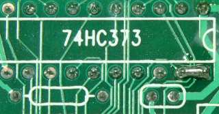
It's immediately obvious something is wrong with one of the lower address lines, because bytes change unexpectedly upon pressing CTRL-L. But this display would lead you to believe that A1 is stuck, because the pattern repeats ever 2nd byte.

In fact, the A1 signal is latched from the D1 signal by the 74HC373. So errors on D1 will cause A1 to be incorrect. Because of this dependance of the address bits on the data lines, the best troubleshooting strategy when mulitple problems are present is to fix the easier data bit problems first, then concentrate on the address bits once the data bits are working properly.

Case 6: Wrong Chip Selected

Most of the signals are address and data lines, so an error at some random position on the board is most likely to impact address or data bits. However, all the memory devices require chip select and control signals, which can also have problems.

This example shows an unlikely problem with chip selects, and also serves to illustrate some properties of the 82C55 peripheral chip.

photo: pins shorted
Figure 5: 74HC138 Enable Shorted To Ground (Always Enabled)

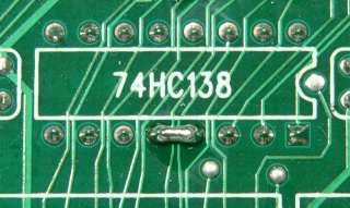
In this sample, the error is a short between pins 4 and 5 of the 74HC138 chip, which forces the output of a 74AC20 gate to zero. The result is the flash rom never gets a chip select signal, and instead the 74HC138 chip always attempts to select a peripheral over the range 0x8000 to 0xFFFF, rather than 0xF800 to 0xFFFF.

Before attempting the memory editor, you should notice the following when downloading the three sample files, leading you to believe the RAM and 82C55 (and all connections) are working properly, but you may have a defective flash rom chip.

blink_ram.hex: downloads without errors and runs without problems.

blink_82c55.hex: downloads correctly and LEDs respond properly.

blink_flash.hex: does not download correctly, and strange problems result.

When downloading to the flash, it will seem the flash is partially working but not storing data reliably. Each download attempt can produce slighly different results. If you try this with the flash chip removed, the same thing happens, which is very mysterious.

PAULMON2 Loc:2000 > ^..............
Download completed

Summary:
 14  lines received
 198  bytes received
 89  bytes written
Errors:
 109  bytes unable to write

PAULMON2 Loc:2000 > ^..............
Download completed

Summary:
 14  lines received
 198  bytes received
 93  bytes written
Errors:
 105  bytes unable to write

PAULMON2 Loc:2000 > ^..............
Download completed

Summary:
 14  lines received
 198  bytes received
 93  bytes written
Errors:
 105  bytes unable to write

PAULMON2 Loc:2000 > ^..............
Download completed

Summary:
 14  lines received
 198  bytes received
 92  bytes written
Errors:
 106  bytes unable to write

When you run the memory editor to begin investigating the problems with the flash rom, unlike usual, the initial screen gives the immediate impression that something is very wrong. It seems as if all the address bits except for A0 and A1 are not working.

CODE        8051 External Memory Editor, Paul Stoffregen, 1996
ADDR: +0 +1 +2 +3 +4 +5 +6 +7 +8 +9 +A +B +C +D +E +F   ASCII EQUIVILANT
------------------------------------------------------------------------
F000: 79 3D E0 E0 79 3D E0 E0 79 3D E0 E0 79 3D E0 E0   y=``y=``y=``y=``
F010: 79 3D E0 E0 79 3D E0 E0 79 3D E0 E0 79 3D E0 E0   y=``y=``y=``y=``
F020: 79 3D E0 E0 79 3D E0 E0 79 3D E0 E0 79 3D E0 E0   y=``y=``y=``y=``
F030: 79 3D E0 E0 79 3D E0 E0 79 3D E0 E0 79 3D E0 E0   y=``y=``y=``y=``
F040: 79 3D E0 E0 79 3D E0 E0 79 3D E0 E0 79 3D E0 E0   y=``y=``y=``y=``
F050: 79 3D E0 E0 79 3D E0 E0 79 3D E0 E0 79 3D E0 E0   y=``y=``y=``y=``
F060: 79 3D E0 E0 79 3D E0 E0 79 3D E0 E0 79 3D E0 E0   y=``y=``y=``y=``
F070: 79 3D E0 E0 79 3D E0 E0 79 3D E0 E0 79 3D E0 E0   y=``y=``y=``y=``
F080: 79 3D E0 E0 79 3D E0 E0 79 3D E0 E0 79 3D E0 E0   y=``y=``y=``y=``
F090: 79 3D E0 E0 79 3D E0 E0 79 3D E0 E0 79 3D E0 E0   y=``y=``y=``y=``
F0A0: 79 3D E0 E0 79 3D E0 E0 79 3D E0 E0 79 3D E0 E0   y=``y=``y=``y=``
F0B0: 79 3D E0 E0 79 3D E0 E0 79 3D E0 E0 79 3D E0 E0   y=``y=``y=``y=``
F0C0: 79 3D E0 E0 79 3D E0 E0 79 3D E0 E0 79 3D E0 E0   y=``y=``y=``y=``
F0D0: 79 3D E0 E0 79 3D E0 E0 79 3D E0 E0 79 3D E0 E0   y=``y=``y=``y=``
F0E0: 79 3D E0 E0 79 3D E0 E0 79 3D E0 E0 79 3D E0 E0   y=``y=``y=``y=``
F0F0: 79 3D E0 E0 79 3D E0 E0 79 3D E0 E0 79 3D E0 E0   y=``y=``y=``y=``
------------------------------------------------------------------------
^E-Edit  ^G=Goto  ^C=Code  ^D=Data  ^L=Redraw  ^Q=Quit

If you try editing this, you will find that locations F000, F001 and F002 appear to be working memory, but F003 does not. If you press CTRL-L before editing F003, your impression that only A0 and A1 is reinforced because the whole screen changes.

If you edit F003 (which does not read back correctly) and then press CTRL-L, all the bytes change to zero.

This is the correct behavior of the 82C55 peripheral chip. The "+3" location is the write-only configuration register. When it is written, the 82C55 chip clears the other three registers to zero. The other 3 bytes are read/write registers that control ports A, B and C.

The important point is to recognize that memory mapped peripheral chips like the 82C55 have very unusual behavior when you are expecting ordinary memory. These chips usually only have a small group of registers (4 in the 82C55), so they appear repeated over and over again in memory. This is not bad address bits.

Recognizing this behavior as the 82C55 chip is the critical step that will lead you to troubleshoot the address decoding logic. It appears at first that the flash chip is defective, but in fact it is most likely perfectly fine, but not actually being used because of an error in the chip selection based on the address bits.

Case 7: No Chip Selected

One final case to be aware of is the circumstance where no chip is responding. This is easy to recognize, because each byte reads the same as its lower 8 address bits, and all attempts to write have no effect.

When you see this in the memory editor, and all attempts to edit have no effect, there is probably no chip being selected.

CODE        8051 External Memory Editor, Paul Stoffregen, 1996
ADDR: +0 +1 +2 +3 +4 +5 +6 +7 +8 +9 +A +B +C +D +E +F   ASCII EQUIVILANT
------------------------------------------------------------------------
FF00: 00 01 02 03 04 05 06 07 08 09 0A 0B 0C 0D 0E 0F                   
FF10: 10 11 12 13 14 15 16 17 18 19 1A 1B 1C 1D 1E 1F                   
FF20: 20 21 22 23 24 25 26 27 28 29 2A 2B 2C 2D 2E 2F    !"#$%&'()*+,-./
FF30: 30 31 32 33 34 35 36 37 38 39 3A 3B 3C 3D 3E 3F   0123456789:;<=>?
FF40: 40 41 42 43 44 45 46 47 48 49 4A 4B 4C 4D 4E 4F   @ABCDEFGHIJKLMNO
FF50: 50 51 52 53 54 55 56 57 58 59 5A 5B 5C 5D 5E 5F   PQRSTUVWXYZ[\]^_
FF60: 60 61 62 63 64 65 66 67 68 69 6A 6B 6C 6D 6E 6F   `abcdefghijklmno
FF70: 70 71 72 73 74 75 76 77 78 79 7A 7B 7C 7D 7E 7F   pqrstuvwxyz{|}~ 
FF80: 80 81 82 83 84 85 86 87 88 89 8A 8B 8C 8D 8E 8F                   
FF90: 90 91 92 93 94 95 96 97 98 99 9A 9B 9C 9D 9E 9F                   
FFA0: A0 A1 A2 A3 A4 A5 A6 A7 A8 A9 AA AB AC AD AE AF    !"#$%&'()*+,-./
FFB0: B0 B1 B2 B3 B4 B5 B6 B7 B8 B9 BA BB BC BD BE BF   0123456789:;<=>?
FFC0: C0 C1 C2 C3 C4 C5 C6 C7 C8 C9 CA CB CC CD CE CF   @ABCDEFGHIJKLMNO
FFD0: D0 D1 D2 D3 D4 D5 D6 D7 D8 D9 DA DB DC DD DE DF   PQRSTUVWXYZ[\]^_
FFE0: E0 E1 E2 E3 E4 E5 E6 E7 E8 E9 EA EB EC ED EE EF   `abcdefghijklmno
FFF0: F0 F1 F2 F3 F4 F5 F6 F7 F8 F9 FA FB FC FD FE FF   pqrstuvwxyz{|}~ 
------------------------------------------------------------------------
^E-Edit  ^G=Goto  ^C=Code  ^D=Data  ^L=Redraw  ^Q=Quit                  

You might expect to see all bytes with the same value, but that is not the way the hardware works. Because of the multiplexing of the lower 8 address bits with the data lines, the 8051 drives the data bus with the lower half of the address. Then when it reads the bus less than one microsecond later, the lines are "floating", with their capacitance charged (or discharged) to the same voltage that was used during the address output to the 74HC373. The result is the display you see here. Recognizing this condition can help you quickly know what is (or isn't) wrong when you see it.

No (or very few) Easy Answers

Troubleshooting memory problems is frustrating. There are no simple, easy tests that quickly diagnose all types of problems.

By downloading to each type of memory, both with and without the other memory chips installed, you can get some initial impressions about whether the chips are working. But as the chip select example (case 6) shows, even that simple technique can be deceptive.

Most memory errors are easy to spot in the memory editor once you start writing to the memory. Pressing CTRL-L to refresh the screen is a critically important step, because address line problems manifest themselves as other related locations unexpectedly changing. Data line problems cause address problems due to the mulitplexed bus, so simpler data bit problems should be solved first before address lines.

Reversing the process shown here, where you can see the incorrect behavior and need to deduce the hardware cause requires good knowledge of the schematic, strong deductive reasoning, and sometimes dumb luck. Often, after staring at the incorrect on-screen performance, taking a break or even "sleeping on it" can help give you a fresh perspective to recognize what it really means.

Hopefully this page has at least illustrated the process (if in reverse) and shown some of the more common problems.

Technical Support

PJRC does not provide technical support for boards built using components purchased from other companies. The text of this page is the only assistance available if your board is hand wired on a breadboard, or using point to point solder or wire-wrap construction.

However, if you built a board from the unassembled kit and it has memory access problems, perhaps we can help. Usually there is a fee for repair to boards build from kits, but it is much less expensive than buying a whole new board.

All assembled and tested boards sold by PJRC should not have memory problems. Assembled boards (with the green dot on the serial port) are fully tested and the circuitry is known to be good before they are shipped. Damaged boards can be repaired simply by replacing the chips. Difficult memory editor techniques are rarely needed for the assembled boards.


8051 Development System Circuit Board, Paul Stoffregen
http://www.pjrc.com/tech/8051/board5/memory_check.html
Last updated: March 3, 2005
Status: finished
Suggestions, comments, criticisms: <paul@pjrc.com>