|
|
FPGA Source Schematics
You do not need these schematic to use or
build the MP3 player.
This page has all of the schematic source needed to recompile the FPGA
configuration files, so that determined hackers can tweak the
circuits implemented inside the FPGA.
Browser-only viewable images are also provided
here for those who are simply curious about what is going on inside
the FPGA.
These schematics are compiled by the
Xilinx "Foundation" software into a file called "mp3.bit", which is then
translated into "mp3.mcs.master" that is included in the firmware
source code. When the firmware is compiled, the contents of
"mp3.mcs.master" are copied into "mp3player.hex", which is the
file you download to program/upgrade the firmware on the board.
Each time the board boots, the 87C52 processor programs the
Xilinx XCS10XL FPGA chip with the "mp3.mcs.master" data that is
part of the firmware image stored in the 39LF010 Flash ROM.
The XCS10XL is not programmed on an
EPROM programmer (it has no permanent memory inside).
When the firmware loads the config data, the
FPGA implements all the circuitry which interfaces the DRAM,
IDE drive, and STA013 MP3 decoder to the 87C52 microcontroller
with paged memory and multiple DMA channels. If you want to
hack on these circuits, or just see what they look like, this is
the page for you. If you just want to make a working player,
you might want to skip this page instead of risking
"information overload".
GNU General Public License
These schematics are Copyright PJRC.COM, LLC 2000, 2001, 2000.
You may redistribute and/or modify these schematics under the
terms and conditions of the GNU General Public License as published by
the Free Software Foundation; version 2.
These FPGA schematics are distributed in the hope that it will be useful
and perhaps even educational,
but WITHOUT ANY WARRANTY; without even the implied warranty of
MERCHANTABILITY or FITNESS FOR A PARTICULAR PURPOSE. See the
GNU General Public License for more details.
Download Files For Xilinx Foundation 3.1i (Aldec Schematics)
- Version 1.16 (2.0M).
-- Corresponds to "mp3.mcs.master" CVS rev 1.16 .
- Version 1.15 (2.0M).
-- Corresponds to "mp3.mcs.master" CVS rev 1.15 .
- Version 1.10 (1.2M).
-- Corresponds to "mp3.mcs.master" CVS rev 1.10 .
This project was designed using schematics. Xilinx Foundation 3.1i
(with Aldec schematic capture) is required to use these schematics.
Update:Tom Parker has been working on translating the
FPGA design to VHDL. Here is
Tom's web page
with his VHDL version.
He also has an archive of emails from
me that explain various parts of the schematics.
Here is a local copy, in
case Tom's website is down.
|
Required Software
These schematics were designed using Xilinx Foundation 3.1i
with service pack 8, using the included Aldec schemtic
capture program. The files will probably be readable
using version 4.1, but I do not have it for testing. The
Aldec schematic software that Xilinx includes is required.
You must also install support for the SpartanXL chips to
be able to compile these schematics into the bitstream.
The free "WebPack ISE" from Xilinx does not include Aldec
and it is also missing support for the SpartanXL chips,
so the free "WebPack ISE" software
will not work. When this project began, the only
low-cost software ($99) was Foundation 3.1i with Aldec.
Xilinx has since discontinued Aldec's schematic capture and
they now provide "WebPack ISE" which is imcompatible with
their previous low-cost software. Complain to Xilinx.
Ultimately, these schematics are compiled into "mp3.bit" by
the Xilinx Foundation software. This file is then translated
into intel-hex using the MakeProm utility. If the MakeProm
splash screen and general slowness annoys you as much as it
does me (and you build the firmware on a linux-based system),
you might try my bit2mcs C code
instead of Xilinx's MakeProm.
The xilinx project was created in the path F:\XILINX\MP3,
where the "MP3.PDF" file (the top-level xilinx file, with
their poor extension choice that conflicts with Adobe
"portable document format") should be in F:\XILINX and the
other files should all go into F:\XILINX\MP3, F:\XILINX\MP3\LIB,
and F:\XILINX\MP3\XPROJ; as indicated by the hierarchy
within the .tar.gz file. It may be possible to build the
FPGA with the files in a different PATH, but this pathname is
embedded within many of the files by the Xilinx tools.
Viewable Images (No Special Software Required)
Warning: these image files are very large. They have been encoded
as 7-color GIF files to speed your download time. To extract these
images from Aldec, I used a postscript print to files and then used
ghostscript to convert to tif and xv to crop and convert to gif.
Saddly, Aldec's printing is buggy (as is just about everything
else about Aldec), so some fonts are incorrectly sized or positioned.
A couple schematics have extra lines where it incorrectly expanded
the lower-right corner title box. There is not much I can do about this.
This list is ordered with the most interesting schematics first
and the really mundane ones at the bottom.
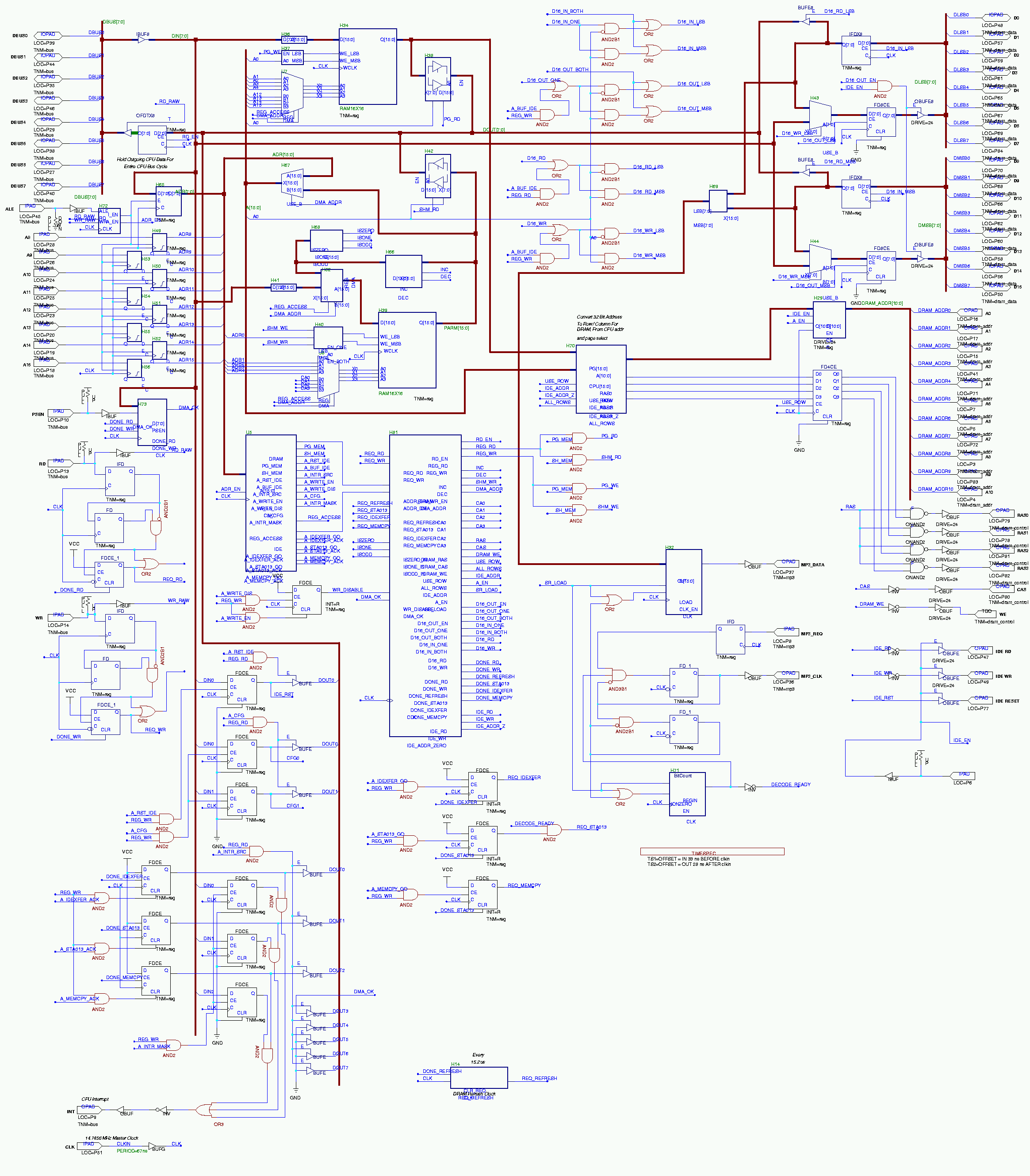
- Main Schematic 1.10 (171k) - This is the complete data path from the 8051 bus to shared parameter/address-mapping memory to DRAM/IDE bus, with all the 8051-visible registers and event detection and action request bits.
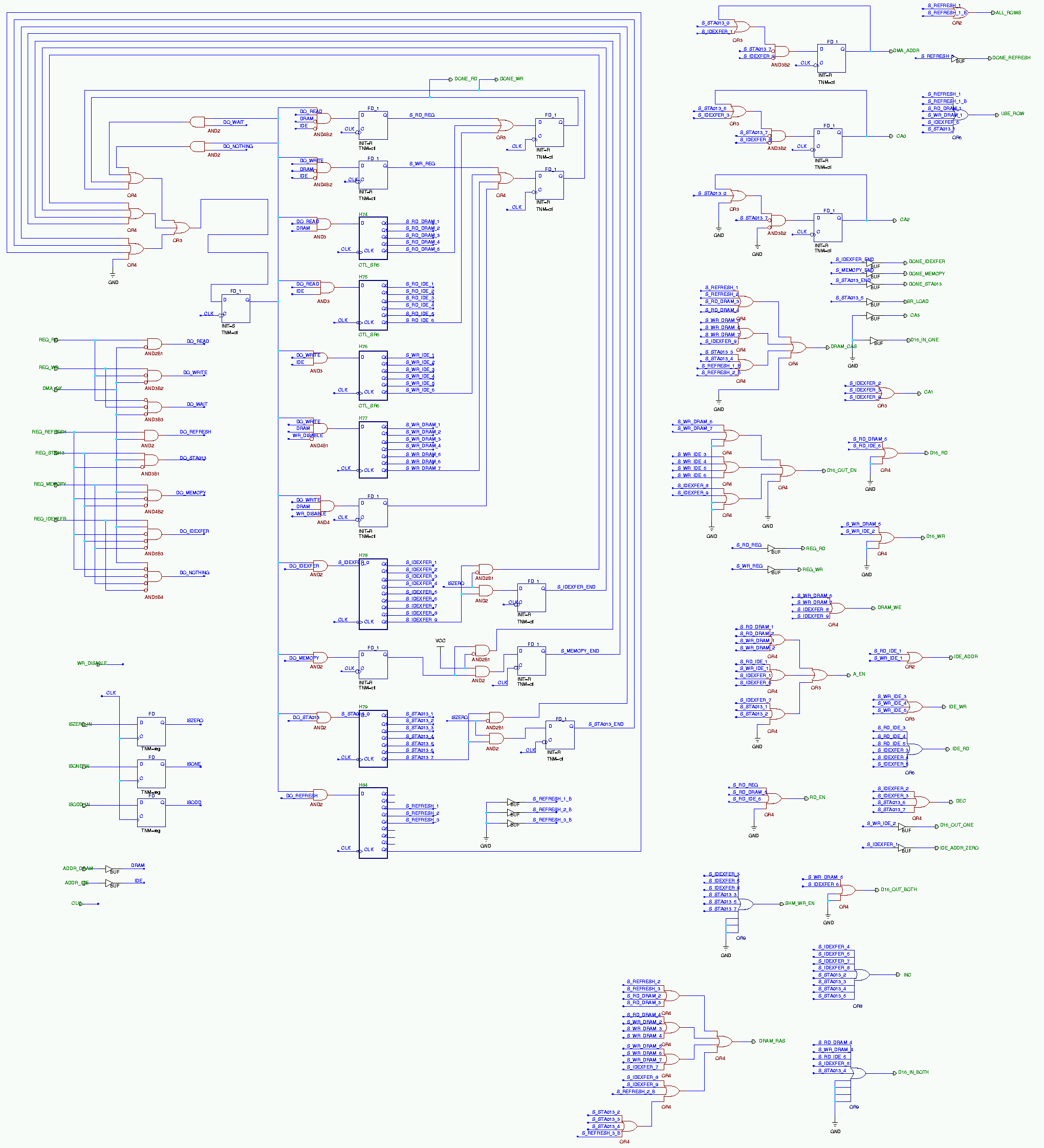
- Control State Machine 1.10 (87k) - Takes the various action request bits and asserts all control lines to cause data to move around. It is a simple (but large) "one-hot" state machine which waits in an idle state until action is needed, and then executes a sequence of states which assert the signals to execute the required data transfer, and then returns to the idle state. Shift register blocks are used to get around memory limits/bugs in Aldec. All states are named with S_state_#, and OR gates assert each control signal during the appropriate states. This schematic also includes the priority encoder which decides what task will run if multiple requests are pending while in the idle state. Though this schematic looks complex, the one-hot idea is for one flip-flop to be high and the others all low, and the "hot" bit travels around. In this schematic, it "stays" at the idle flip-flop until the priority-encoding gates decide to allow something to happen, and then is travels down one of the paths and returns back to the idle state. The DMA paths have one optional flip-flop that gets the "hot" bit if that sequence of states resulted in the condition (ISZERO) that terminates the DMA operation. All control signals are generated by OR gates that simply assert the signal during a group of states, except for a couple timing critical signals which use a set/reset register (equivilant OR gate functionality without the delay).
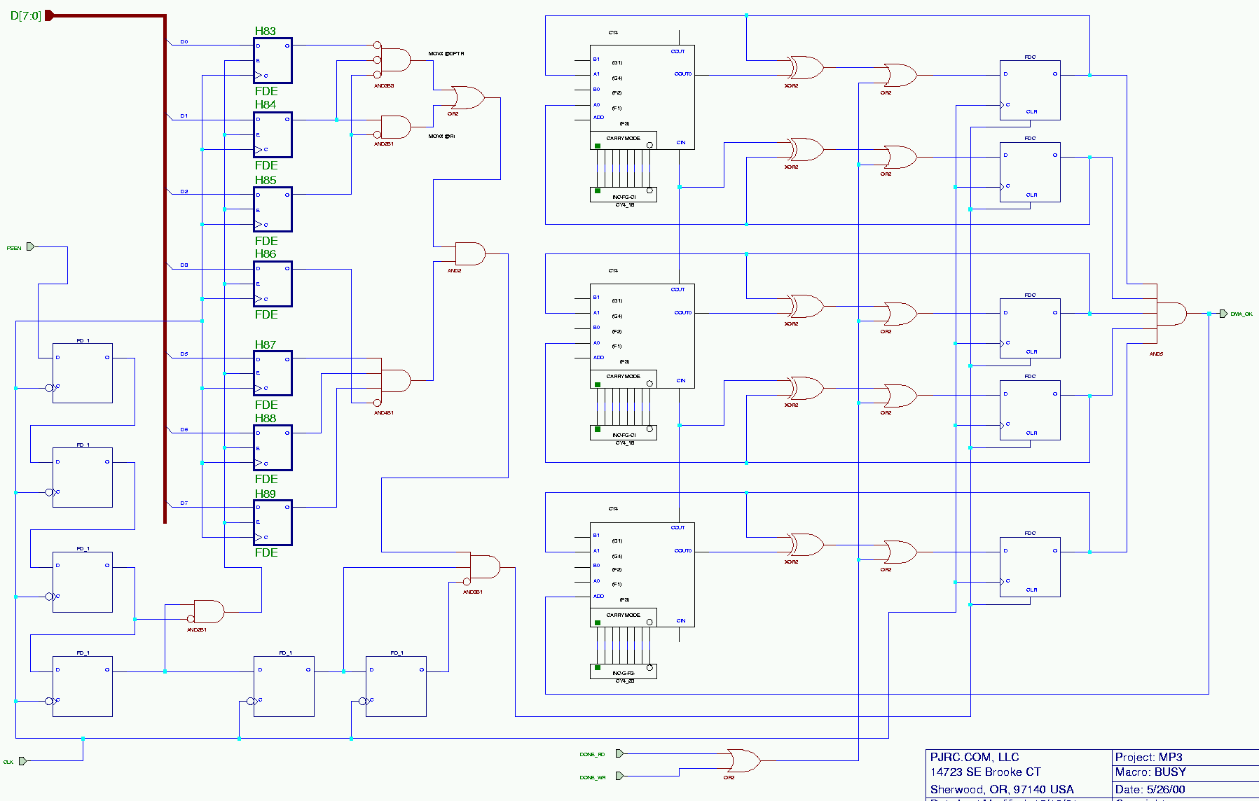
- 8051 Bus MOVX Prediction 1.10 (43k) - Listens to the 8051 bus and asserts DMA_OK when no MOVX instructions are expected. The priority encoder will avoid starting any non-8051 access to the DRAM when DMA_OK is not asserted, so that we will always have low-latency when responding to the 8051's RD and WR requests (which can't be lengthened because the 8051 does not have wait states). A 31-cycle timer re-asserts DMA_OK if a MOVX opcode was seen but no MOVX was performed (operand or data was same byte as MOVX opcode).
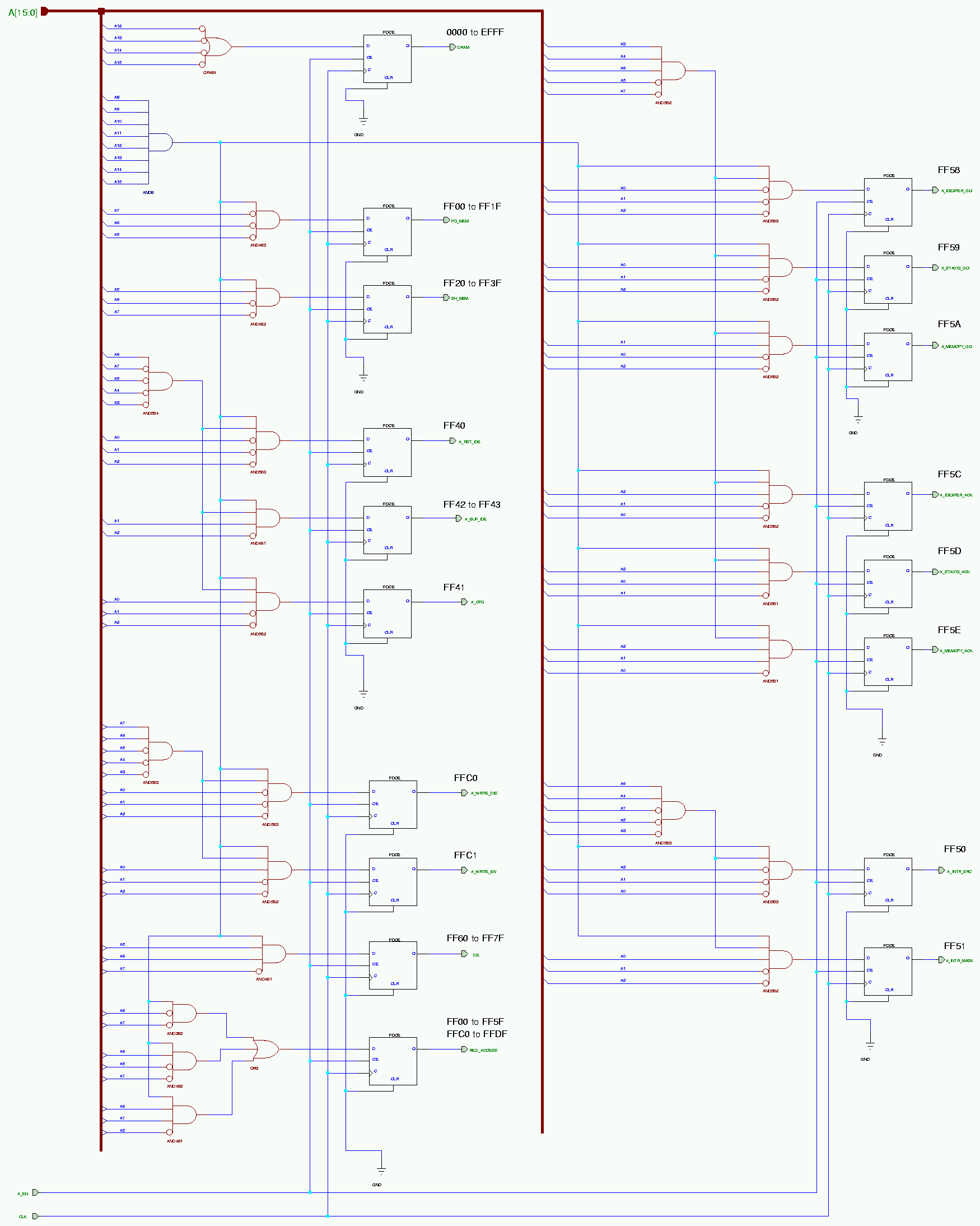
- 8051 Address Decode 1.10 (64k) - Asserts signals for each 8051 register used in the memory map. Usually these are AND'd with REG_RD or REG_WR (when the state machine decides to allocate the buses) to access the 8051-visible registers.
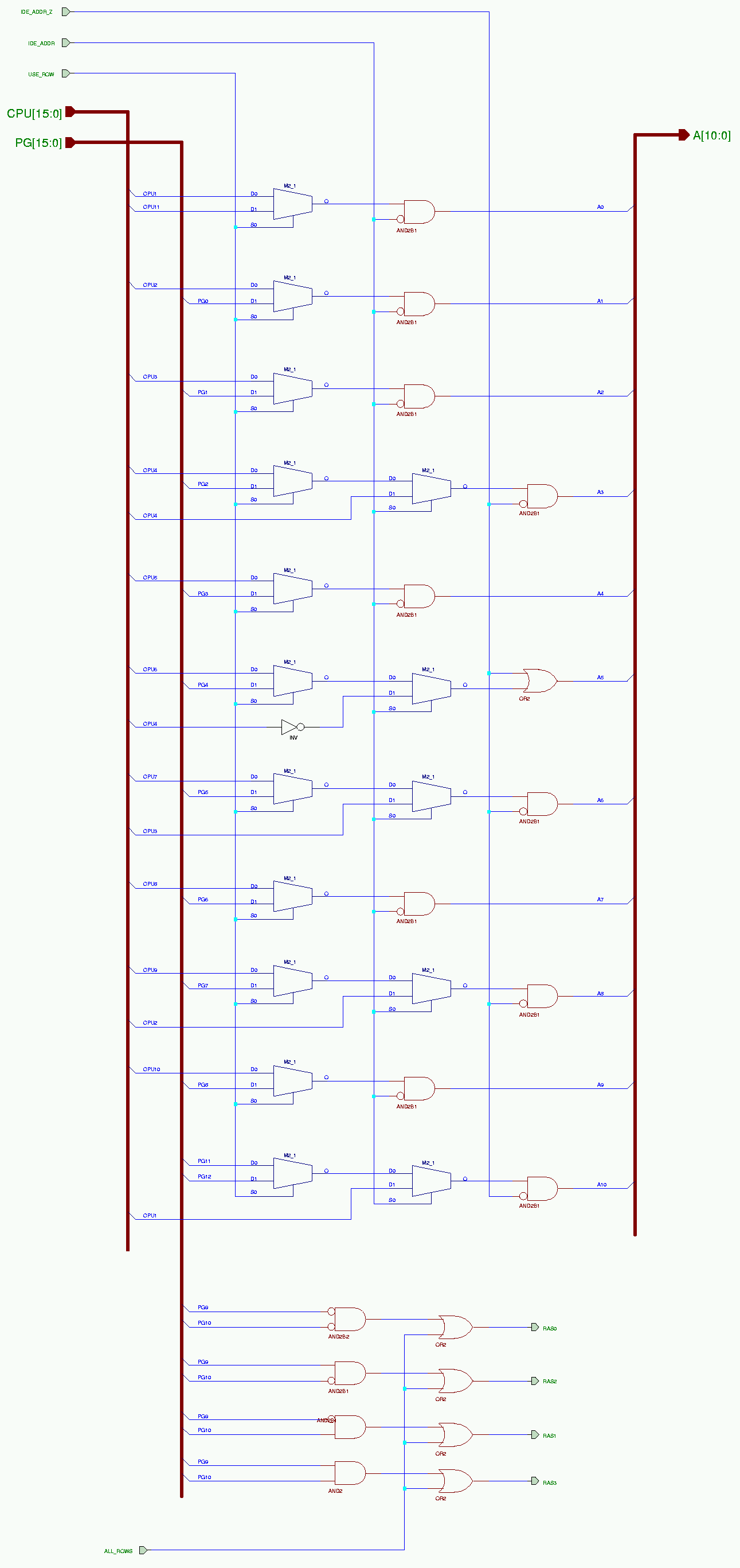
- DRAM/IDE Address Multiplexer 1.10 (47k) - Switches the DRAM/IDE address pins between the row and column address bits for DRAM, address bits for IDE (from 8051), or zero when doing IDE DMA transfers (which look like PIO reads to the drive).
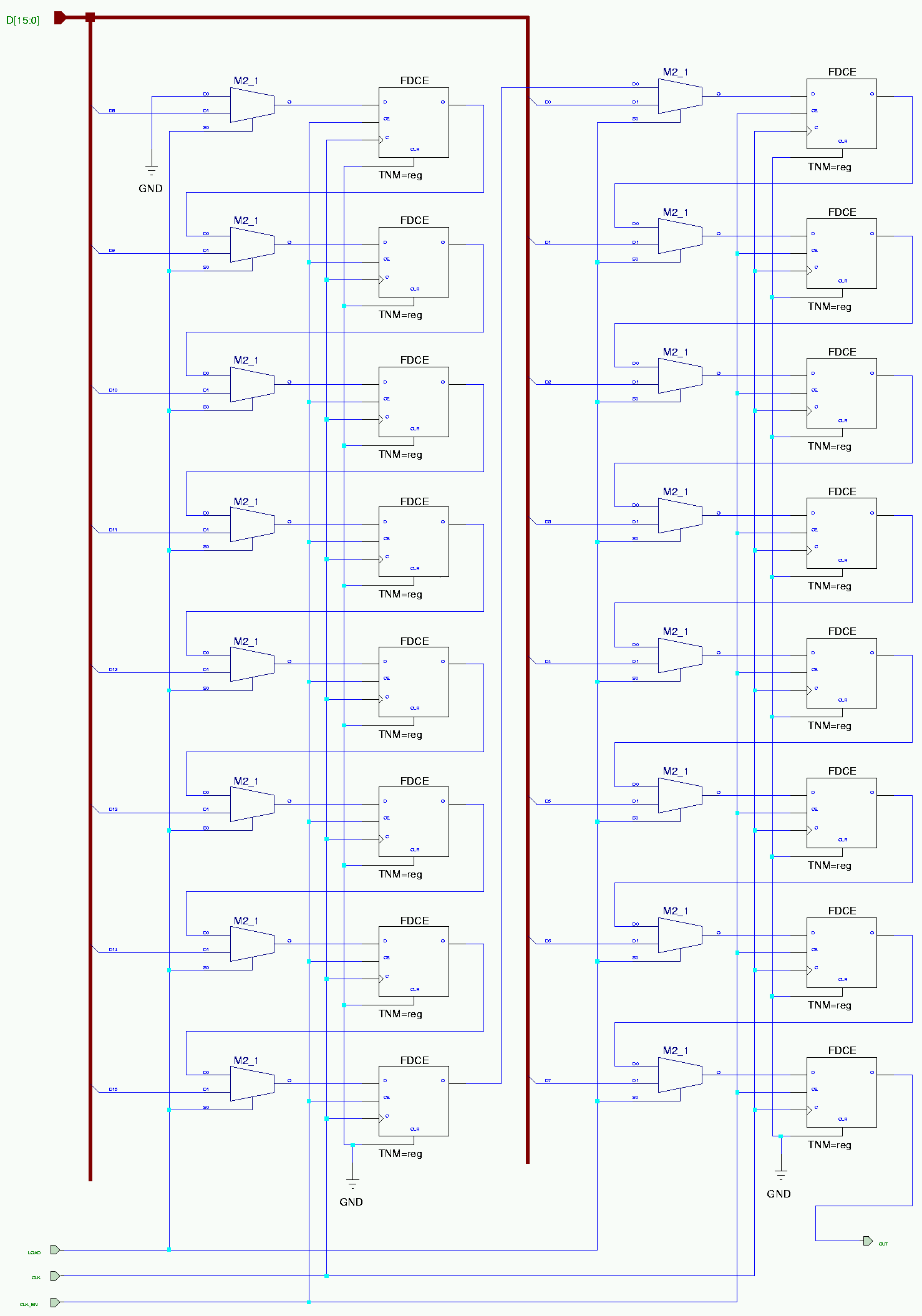
- MP3 Output Shift Register 1.10 (62k) - 16 bit shift register that captures a 16-bit word from the IDE interface and shifts it to the STA013 MP3 decoder.
- MP3 Bit Counter 1.10 (34k) - Counts the number of bits sent by the shift register to the MP3 decoder. A signal is created when all 16 bits have been shifted out and the shift register is ready for the STA013 DMA to transfer another word from DRAM.
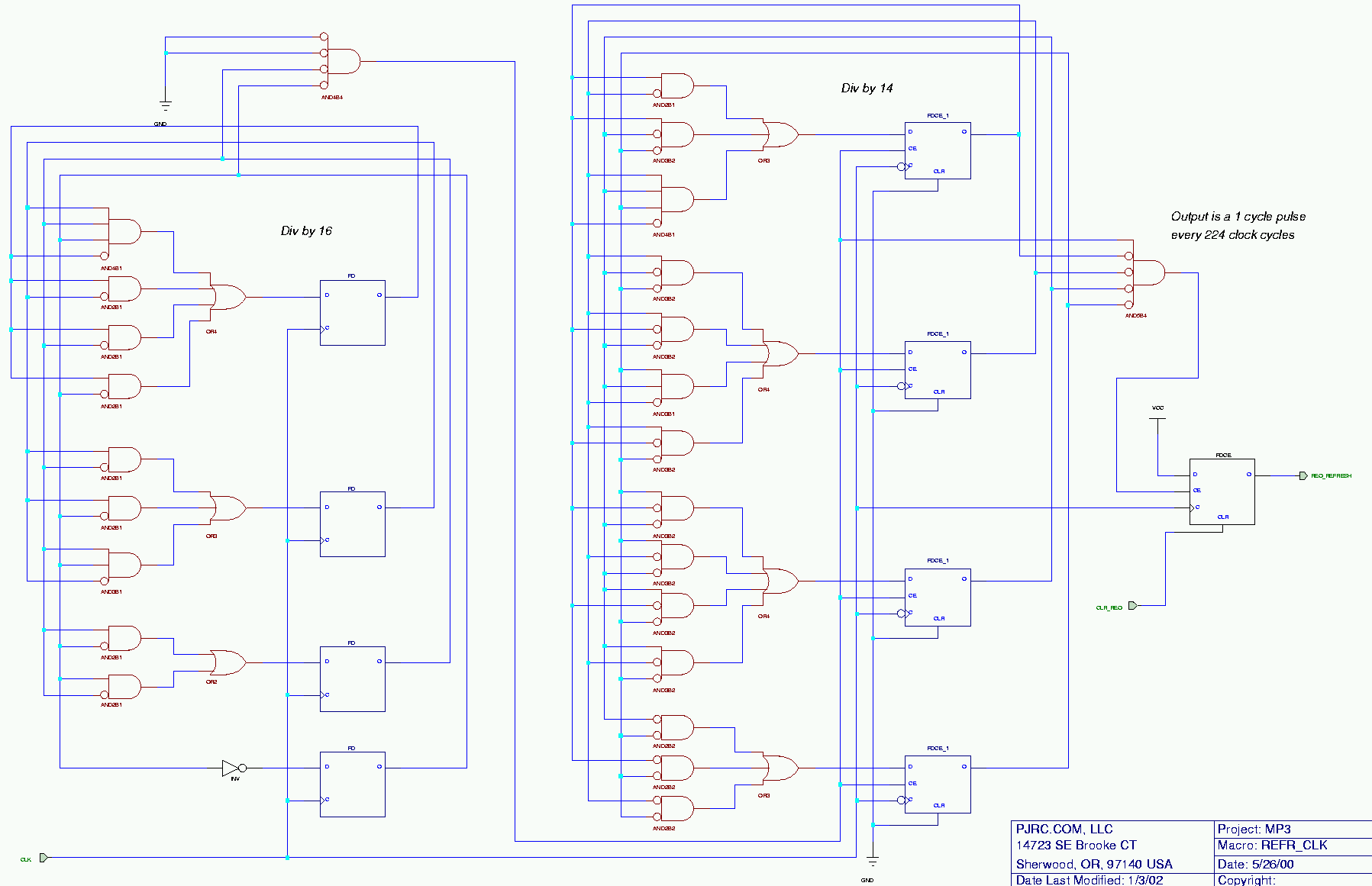
- DRAM Refresh Clock 1.10 (40k) - Generates a pulse every 15.2 µs which creates a request for the state machine to execute a DRAM refresh cycle. This circuit only generates a pulse every 15.2 µs. That pulse sets the request flag on the main schematic, and the control state machine causes the refresh operation to execute when the busses are available and no higher-priority requests are pending.
- DRAM/IDE Address Buffer 1.10 (32k) - Holds the address which is driven to the DRAM and IDE interface.
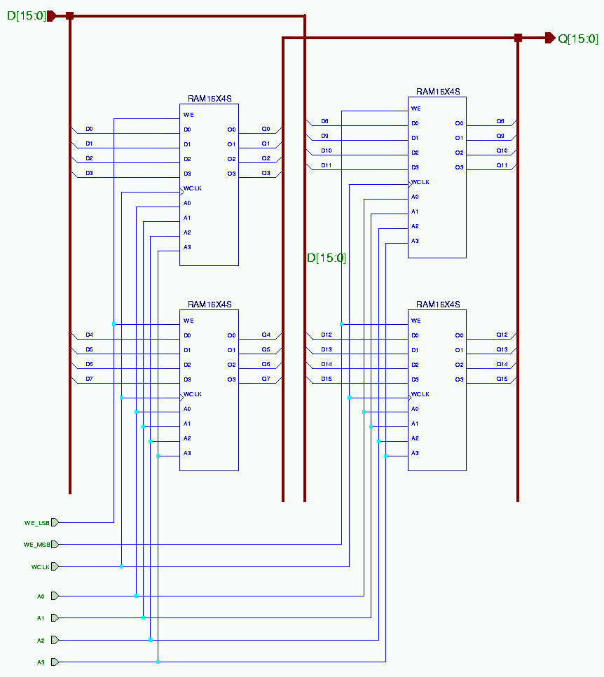
- 32 Byte SRAM Memory 1.10 (20k) - Two of these 16 by 16 bit wide memories are used. One holds the DRAM page numbers that are mapped into the 8051's address space (registers 0xFF00 to 0xFF1F), which are fed to the DRAM/IDE Address Mux together with 12 of the 8051's address bits to create a unique address within the DRAM for every read or write. The second memory RAM holds DMA parameters (registers 0xFF20 to 0xFF3F).
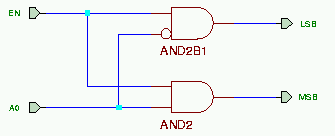
- Write Enable For Address Mapping Memory 1.10 (1k) - Enables the Address Mapping Memory for writing. It can only be written by the 8051 in memory range 0xFF00 to 0xFF1F, so this is a simple circuit to enable the correct half of the memory when the 8051 writes the LSB or MSB.
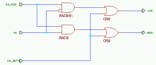
- Write Enable For DMA Parameter Memory 1.10 (2k) - Enables the DMA Parameter Memory for writing. The 8051 can write to these parameters, and they can also be updated by the control state machine through as it changes them during a DMA transfer.
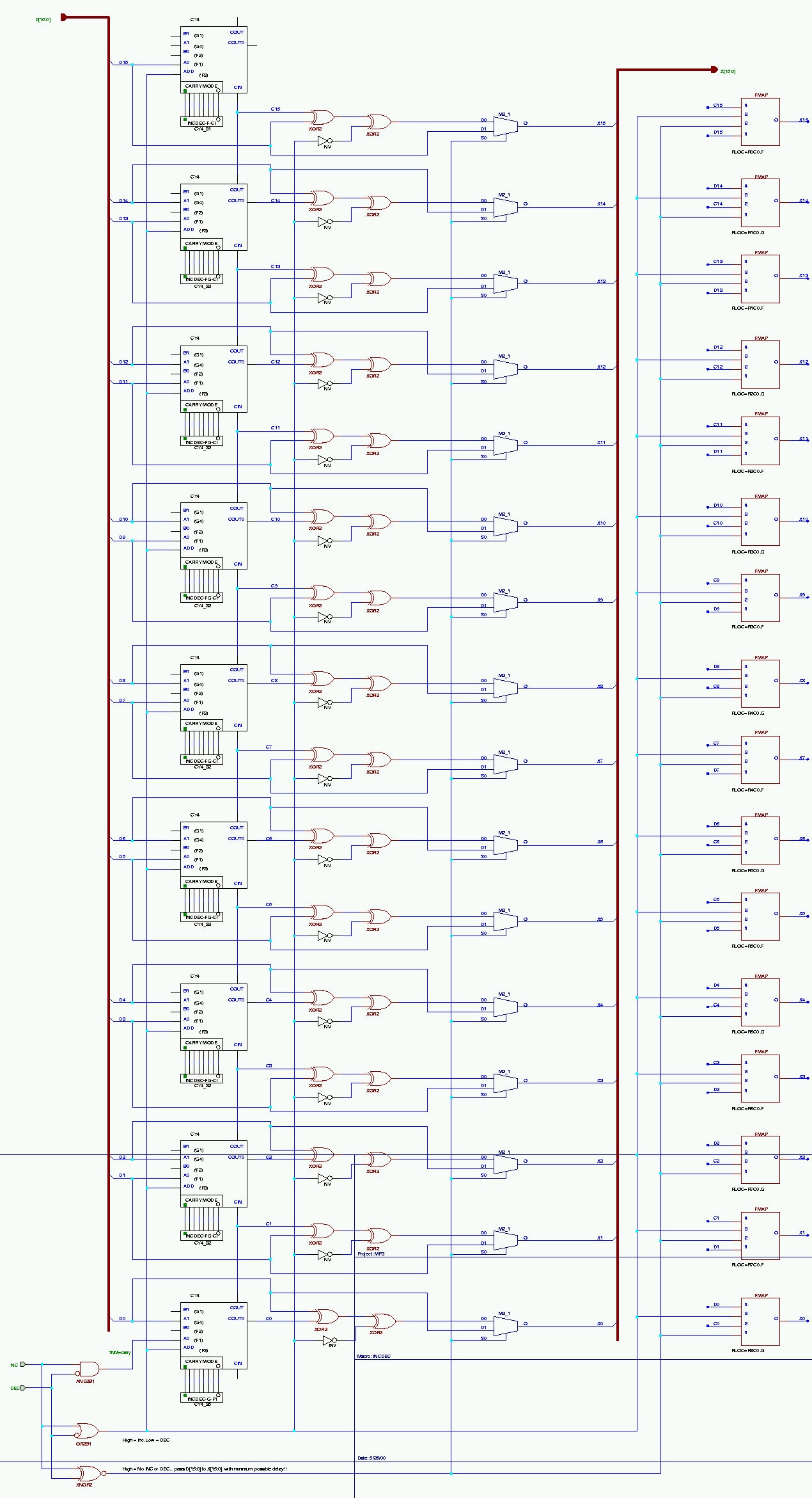
- 16 Bit Increment/Decrement 1.10 (70k) - 16 bit inc/dec used to update stored parameters during DMA transfers (inc for target addresses in DRAM, dec for word count). The output of the DMA Parameter Memory feeds into this circuit, and it also feeds into 16 muxes to allow DMA parameters to become translated into addresses as if they had come from the 8051 address bus.
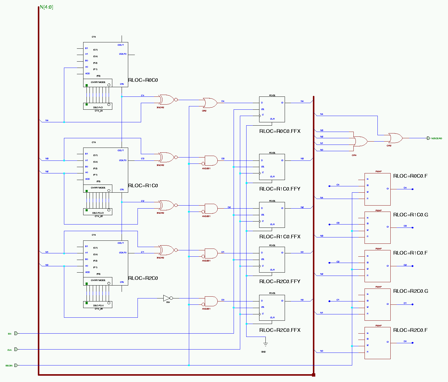
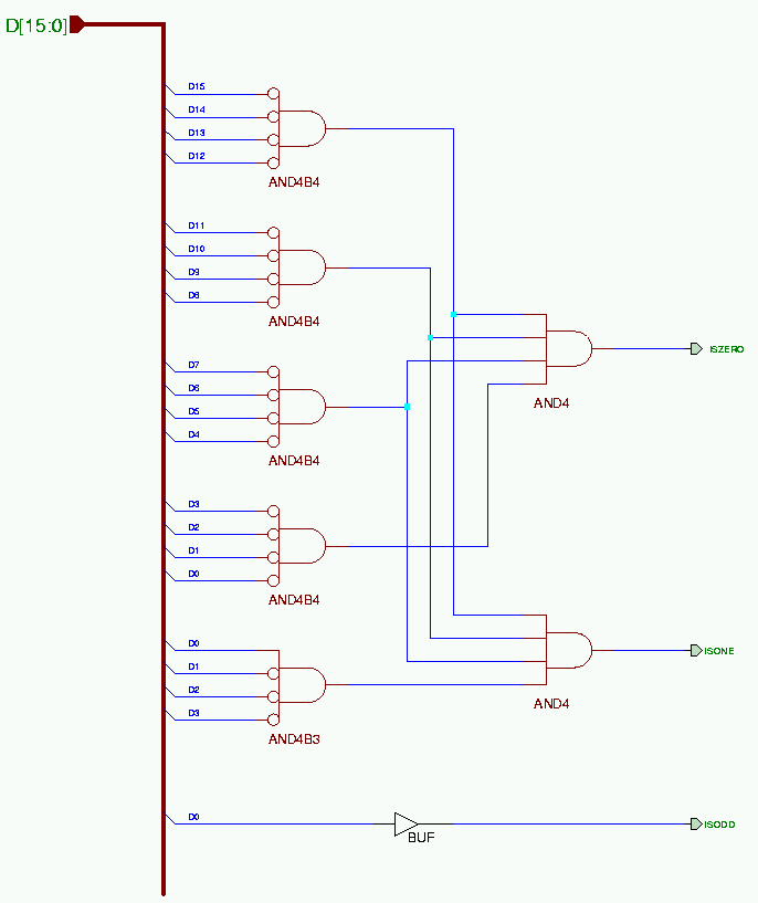
- Zero, One and Odd Number Detector 1.10 (8k) - This circuit monitors the DMA parameters as they are modified and notifies the control state machine if they are zero, one or an odd address. Currently only zero is used by the state machine to know when to clear each DMA request flag to terminate that DMA operation, and set the DMA complete interrupt flag.
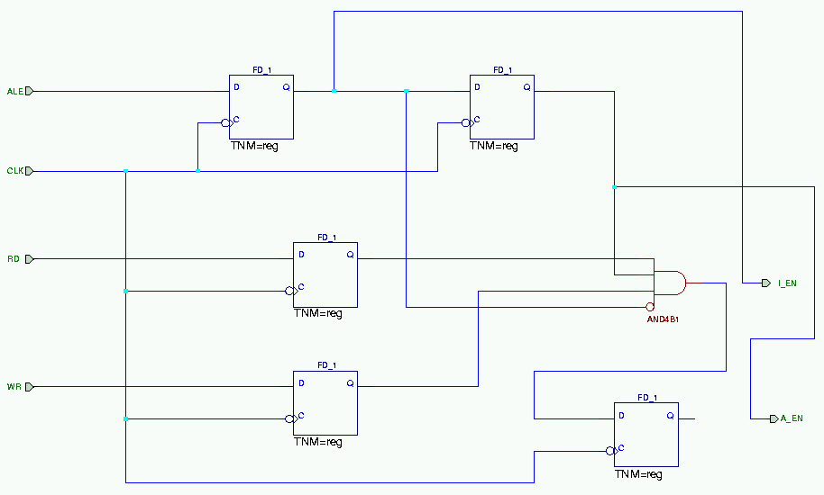
- 8051 ALE Signal Sync 1.10 (7k) - Sync the 8051's ALE signal to the FPGA's clock. Similar sync'ing is done for the other 8051 control signals, but in the main schematic.
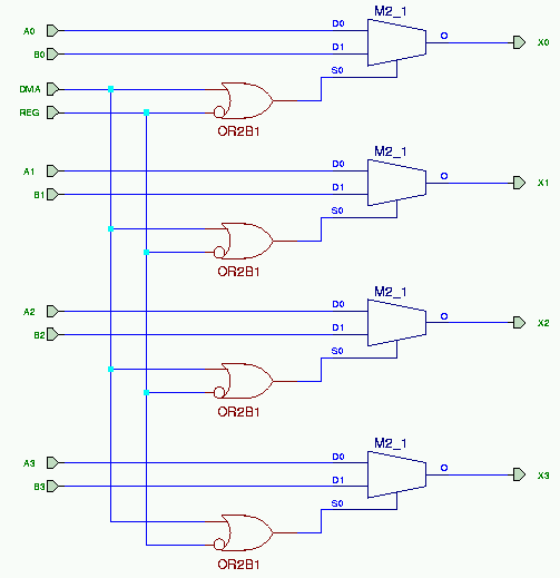
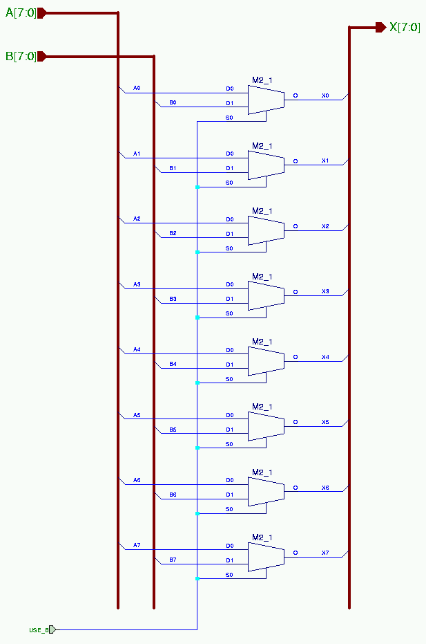
- 2:1 Mux, 4 Bits 1.10 (6k) - These 4 bit muxes allow the address within each of the 32 byte memories to be controlled by their "normal" function, or by the 8051's bus when the firmware read or writes from those registers (to change address mappings or setup DMA transfers).
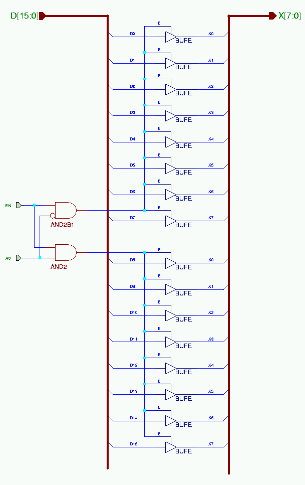
- 2:1 Mux, 8 Bits 1.10 (10k) - Used in the IDE section to allow the output buffers to be loaded from the 8051's data or from what was previously read (is that feature ever used??)
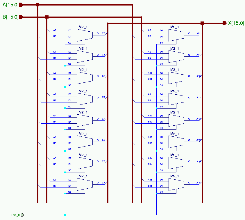
- 2:1 Mux, 16 Bits 1.10 (18k) - Used to switch the address bus from the 8051 (normal operation) to the DMA parameter memory when a DMA cycles is executed.
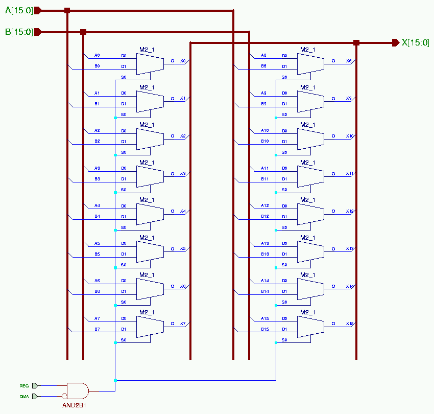
- 2:1 Mux, 16 Bits 1.10 (17k) - Used to switch the DMA parameter memory input between the updated DMA parameters (during a DMA cycle) and the 8051's data bus (when the 8051 writes DMA settings). A separate 16 bit mux is used because Xilinx's CLB mapping will not absorb the extra gate into these 2:1 MUX's (wastes 8 CLBs and adds extra delay in timing critical path) unless it is in the same schematic sheet.
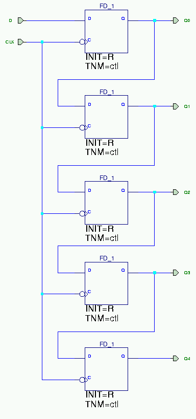
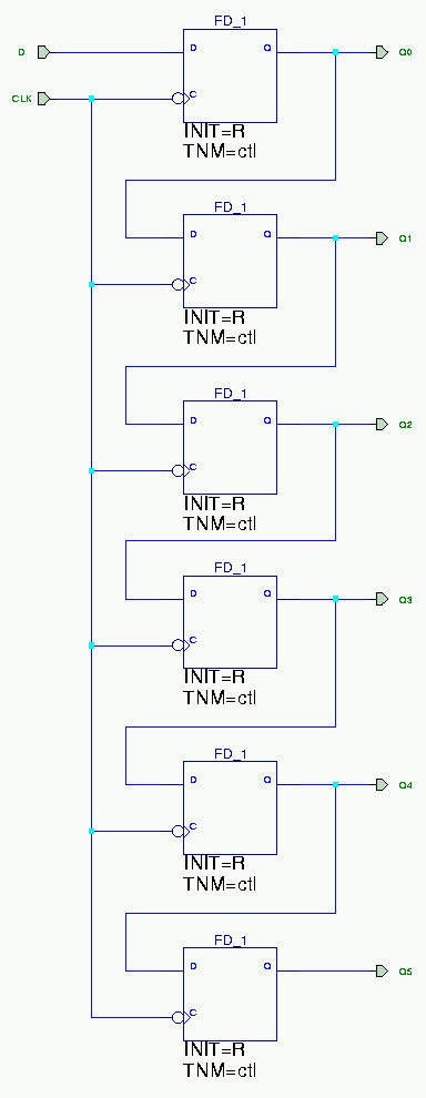
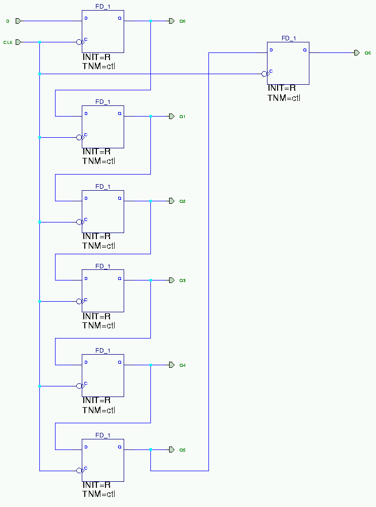
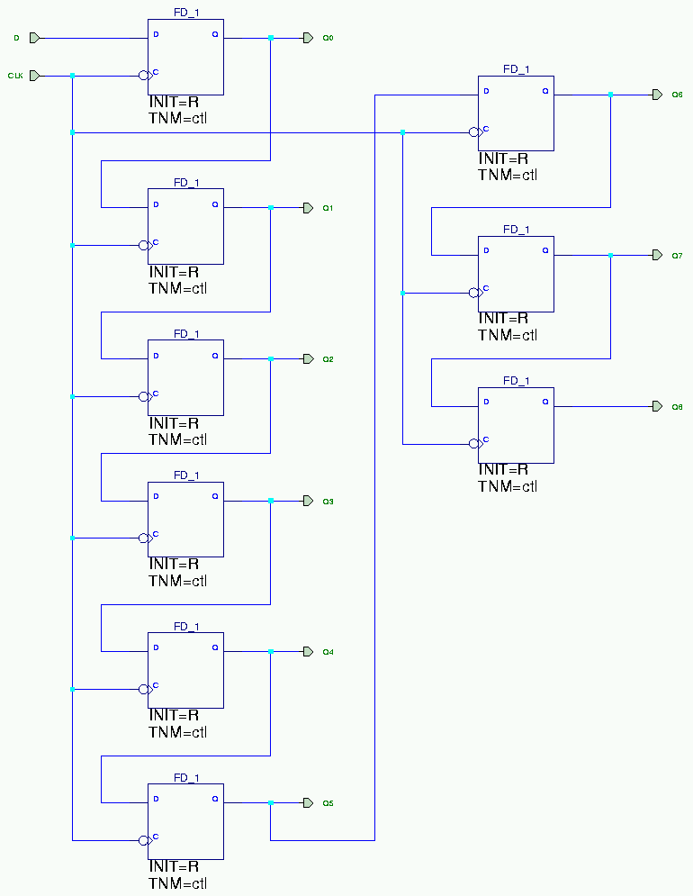
- Shift Register, 5 Bits 1.10 (7k) - Used in state machine. Avoids Aldec crashing due to too many symbols on one sheet.
- Shift Register, 6 Bits 1.10 (8k) - Used in state machine. Avoids Aldec crash.
- Shift Register, 7 Bits 1.10 (10k) - Used in state machine. Avoids Aldec crash.
- Shift Register, 9 Bits 1.10 (13k) - Used in state machine. Avoids Aldec crash. Did I mention yet how buggy Aldec is??
- 16 To 8 Bit Bus Tri-State Buffers 1.10 (11k) - Tri-State buffers to allow either half of a 16 bit
bus to drive an 8 bit bus. Used to allow the 8051 to read from the 16-bit wide memories.
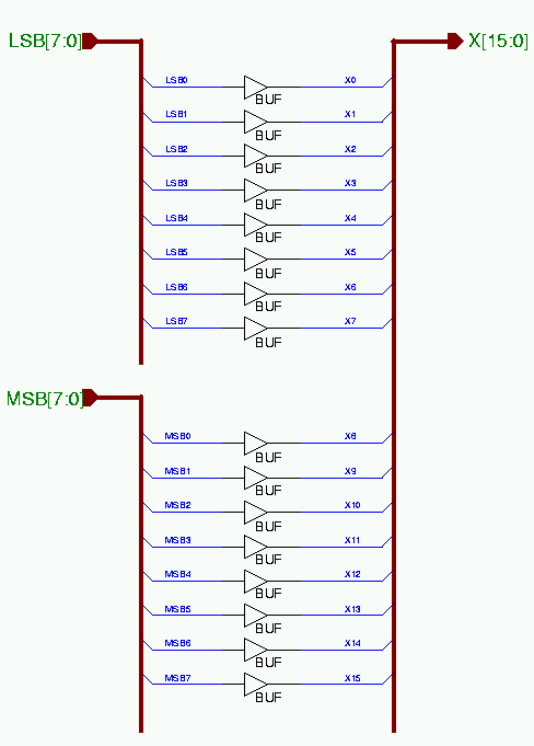
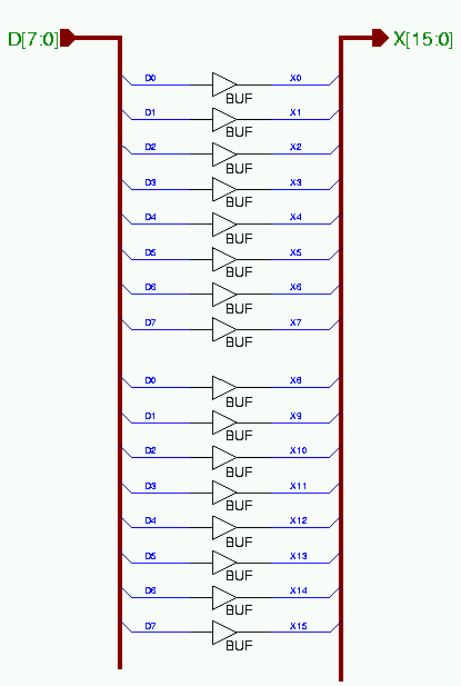
- 8 to 16 Bit Bus Buffer 1.10 (7k) - Connect two 8 bits busses into one 16 bit bus (without Aldec getting confused)
- 8 to 16 Bit Bus Buffer 1.10 (6k) - Connect one 8 bit bus two both halves of a 16 bit bus (without Aldec getting confused)
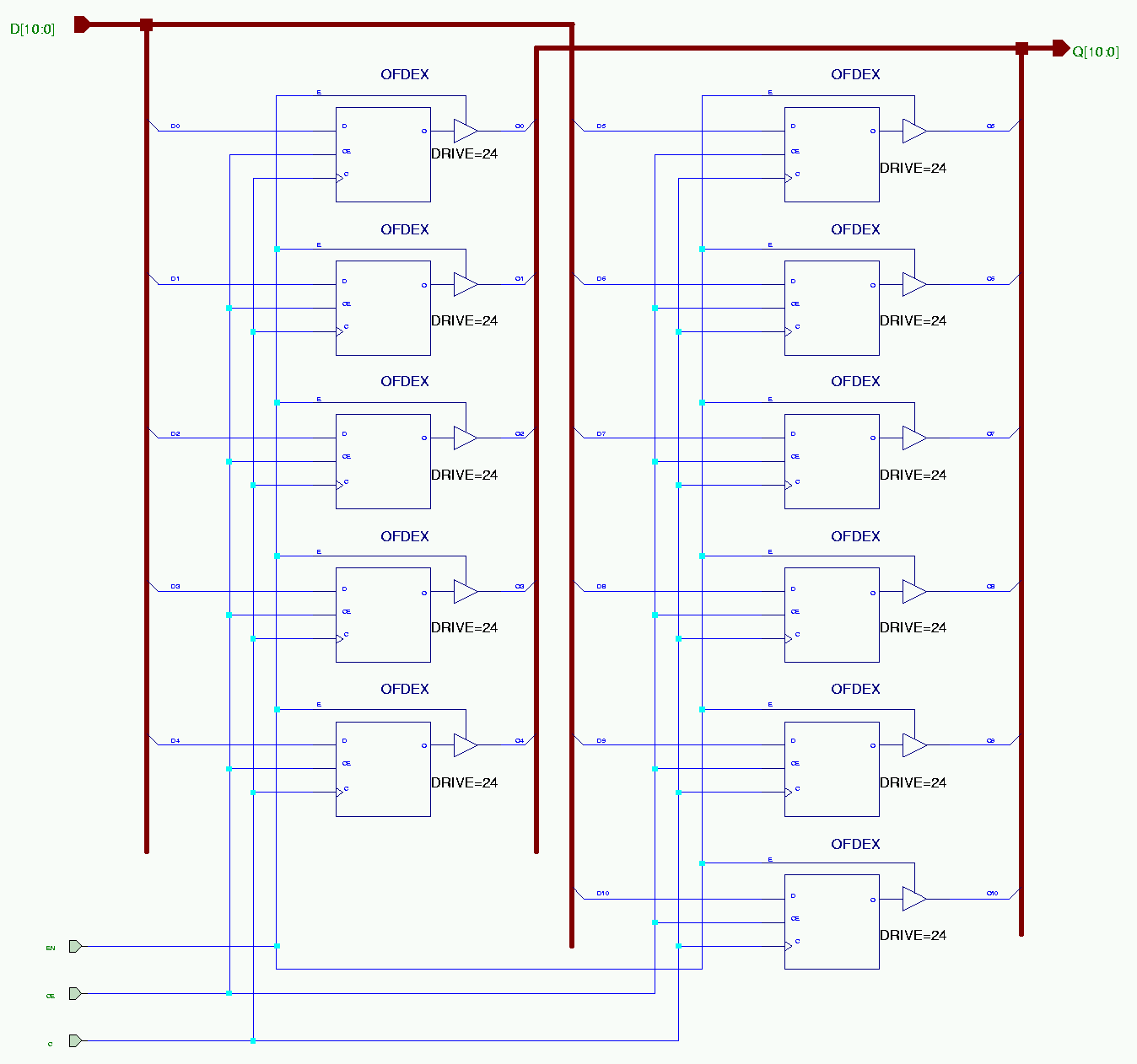
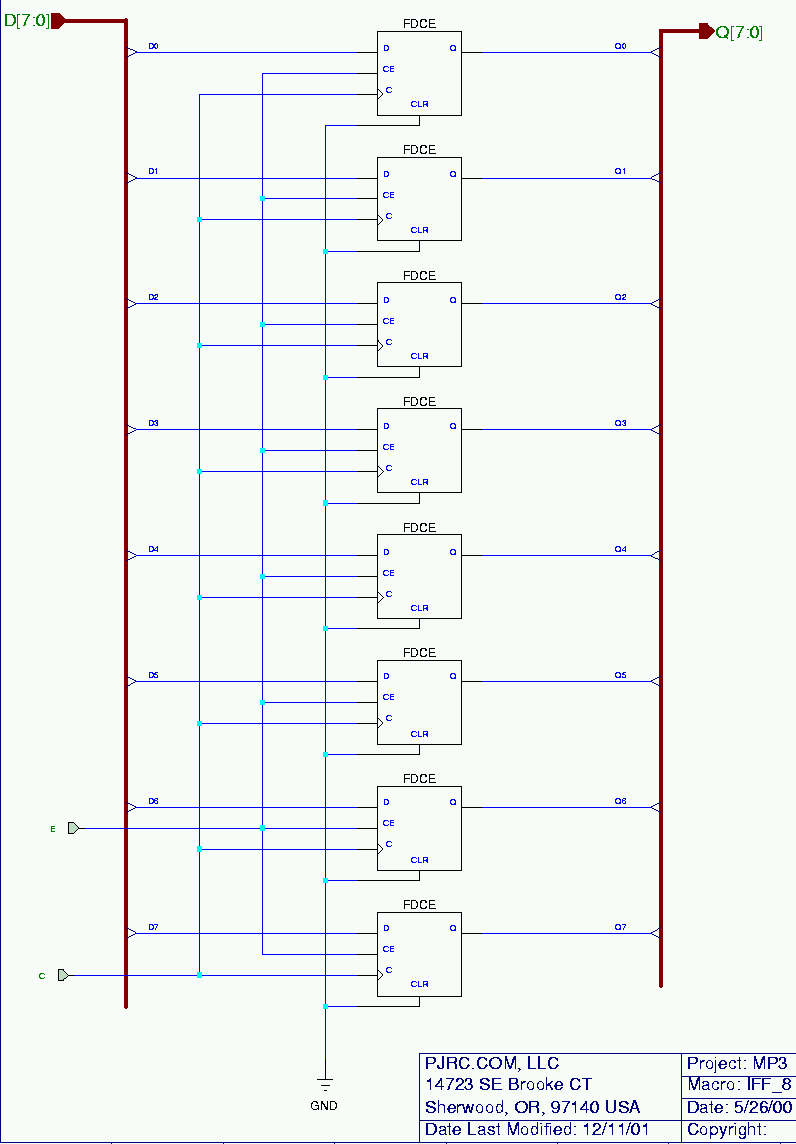
- 8 Bit Register 1.10 (19k) - An 8 bit register, used to capture the 8051's address bits.
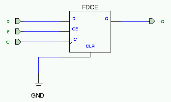
- Flip-Flop (in CLB) 1.10 (1k) - A single CLB flip-flop, redrawn with a smaller symbol than the one in the Xilinx library.
- Flip-Flop (in IOB) 1.10 (1k) - A single IOB flip-flop, redrawn with a smaller symbol than the one in the Xilinx library.
There are a total of 30 schematics. I will eventually convert all
of them to on-line viewable GIFs, in the order that they are interesting.
Several are just boring flip-flops, shift registers, bus buffers, etc; so those will
be done last.
|