|
|
| ||
|
Shopping Cart
|
| Home | Products | Teensy | Blog | Forum |
|
You are here:
MP3 Player
|
|
|
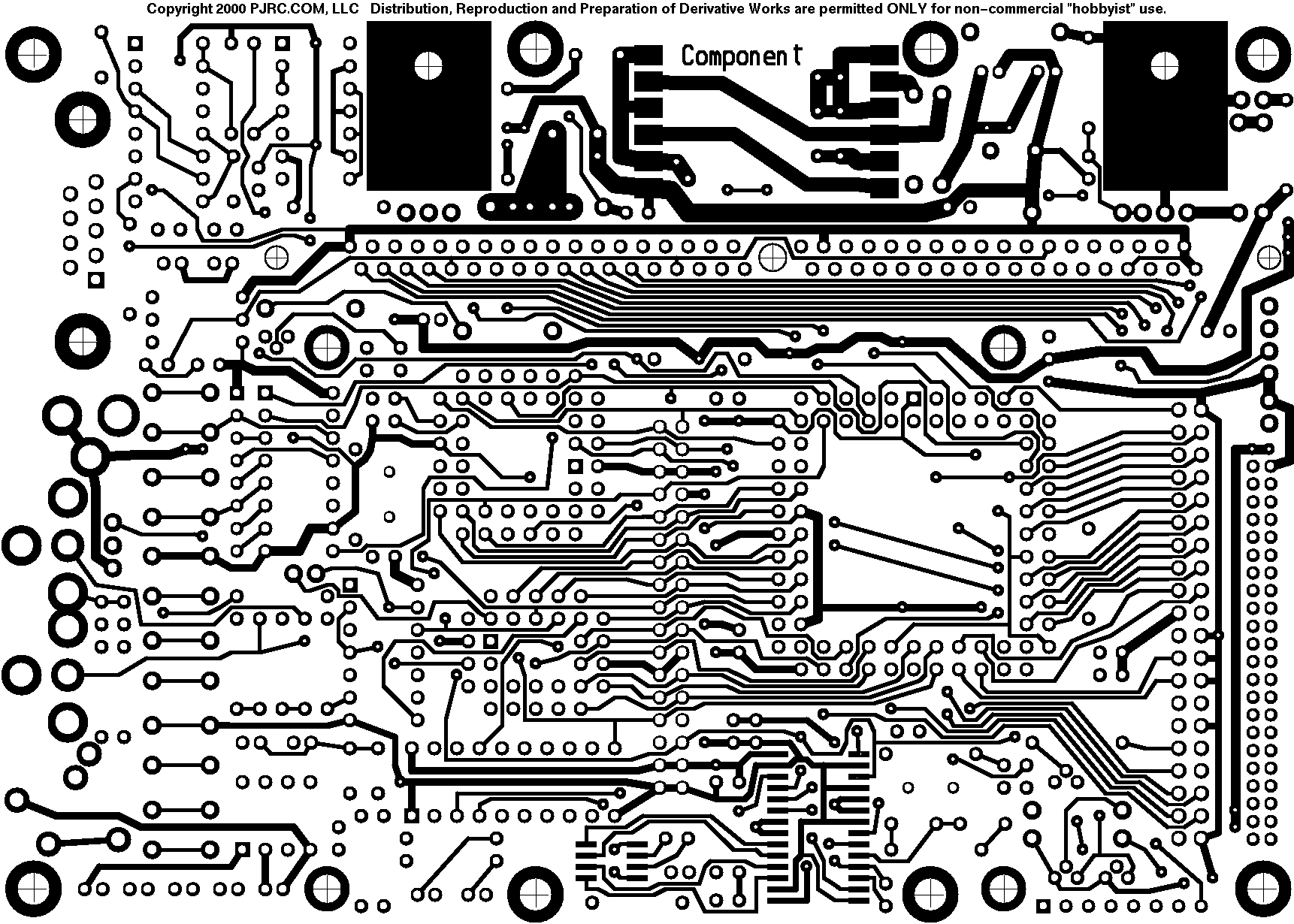
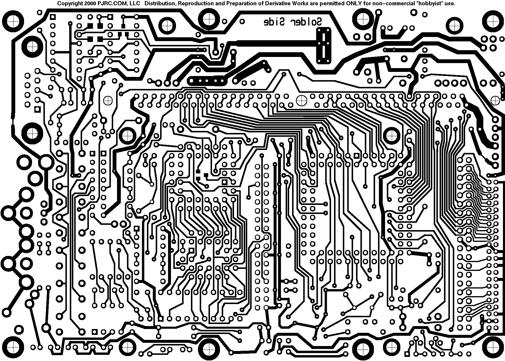
Printed Circuit Board Layout Artwork (Rev A)These printed circuit board images are provided for hobbists who want to attempt etching their own board. They are provided in the hope that they will be useful, but without any warranty; without even the implied warranty of merchantability or fitness for a particular purpose.These images are Copyright PJRC.COM, LLC. Distribution, Reproduction and Preparation of Derivative Works are permitted ONLY for non-commercial "hobbyist" use. No other Distribution, Reproduction or Preparation of Derivative Works is authorized.
To download these images, you may follow the link to each image and select "Save As..." from your browser's File menu. Most browsers also provide an option to save the image in their popup menu, which is access by clicking with the right mouse button (or holding the button for a few seconds on a one-button Macintosh mouse).
Hobbyist Etched Board Assembly TipsIt is possible, though quite difficult, to build this design using a simple home-etch circuit board that lacks plated holes. Here is a photo of my first board, built in this manner:
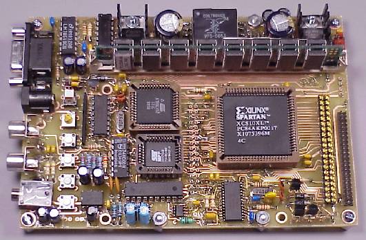 This board differs slightly from rev A, as I discovered a few errors in the layout, which were of course corrected for rev A. Nearly all of the lines on this board are 15 mil (0.015 inch, 0.38 mm) wide, with 10 mil (0.01 inch, 0.25 mm) separation. The only exception is on the solder side where the connections are made to the 44 pin laptop drive connector. The board must be etched with a process that can reproduce 15 mil lines with 10 mil separation. Most hobbyist photoresist-based methods can acheive this if done properly, but iron-on techniques are questionable for this resolution. When assembling the board, many connections are made on the component side of the board. This poses a serious problem for soldering the PLCC sockets and SIMM socket. I used single-pin insert sockets, which are visible in the photo between the microcontroller and flash rom (the two smaller PLCC chips) and the large FPGA chip. They must be soldered on both sides for many locations, and soldering on the top is tricky, as a slight wrong movement will flood the socket with solder. These single-pin inserted sockets are available from Digikey (TODO: find exact part number I used). Unfortunately, they are expensive, but there is little other choice. They also require special PLCC sockets with narrow pins. If you do manage to build the board by etching it yourself, please consider sending a photo or two to add to the User Photo Gallery. |