|
|
| ||
|
Shopping Cart
|
| Home | Products | Teensy | Blog | Forum |
|
You are here:
MP3 Player
|
|
|
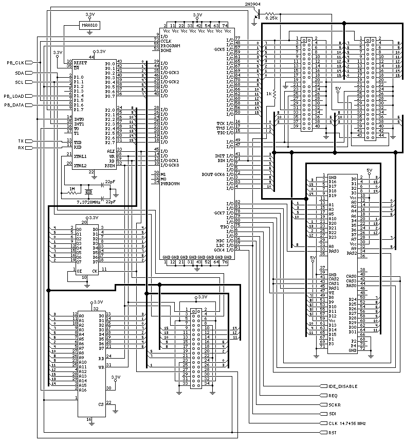
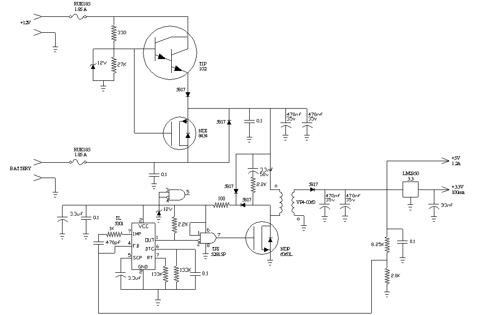
Schematic Diagrams, MP3 Player Circuit Board (Rev C)
Student Project Alert: Many students request this schematic. Many student projects have a scope of work where using this design is legitimate, like this student project where they tried to write ATAPI drivers. For student projects which mandate original hardware design work (not just construction or modification of an existing design), using this large and complex design would be very unwise, as it is more sophisticated than a typical student project. The older design is realistic for a student project. It wouldn't be hard to convert that design to the STA013/CS4334, using the How To Use The STA013 page (that also includes working code).
The schematics on this page describe all of the wiring on the circuit board. Inside inside of the FPGA is described on a separate FPGA schematic page. The circuitry implemented inside the FPGA is configured by the firmware when the board boots, so that circuitry may be changed with the firmware upgrades. The SDA and SCL lines are mis-labeled in figure 1. P1.0 is the SCL signal, and P1.1 is SDA.
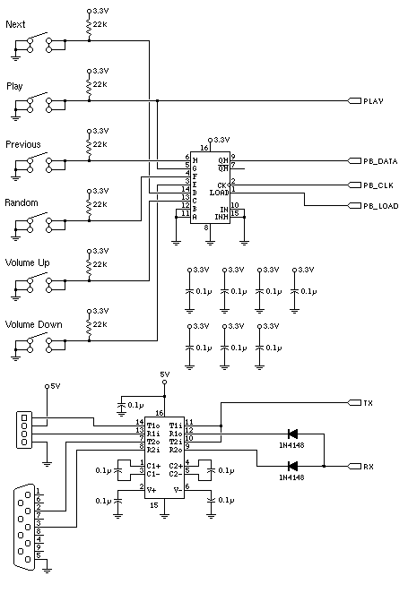
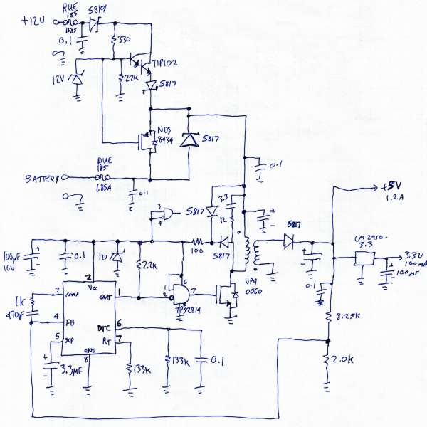
Corrections And Additional InformationFigure 4: Someday this hand-drawn power supply schematic should be replaced with a nice and neat image.Figure 4: The two unspecified polarized capacitors (one directly above the transformer and one directly to the right of the transformer) are actually each a pair of 470 µF capacitors in parallel (for a total of four 470 µF capacitors). These capacitors MUST be Low-ESR types for the power supply to function properly. Figure 4: The two 100 µF 16V capacitors were changed to 33 µF. PJRC provides these as Low-ESR capacitors to reduce noise. Standard capacitors, from 22 µF to 220 µF are likely to work. Figure 4: The capacitor labeled "3.3" (above and to the left of the transformer) is 3.3 nF, or 0.0033 µF. Figure 4: The IC is a TL5001 PWM Controller. The AND gates are TPS2814 MOSFET drivers. Figure 4: The 3.3 µF capacitors attached to pin 5 should be 2.2 µF (either value will work, but we have been using 2.2 µF on the assembled boards and unassembled kits). This capacitor sets the time constant before the power supply will automatically shut off when the output is shorted or the input voltage is too low. Figure 4: The diodes shown connected between the source and drain on the two MOSFET transistors are the diode structures inside transistors. These two diode symbols do not represent actual diode components soldered to the circuit board. Figure 3: The upper chip is 74HC165, and the lower one is MAX232. |