|
|
| ||
|
Shopping Cart
|
| Home | Products | Teensy | Blog | Forum |
|
You are here:
OSU8 Microprocessor
|
|
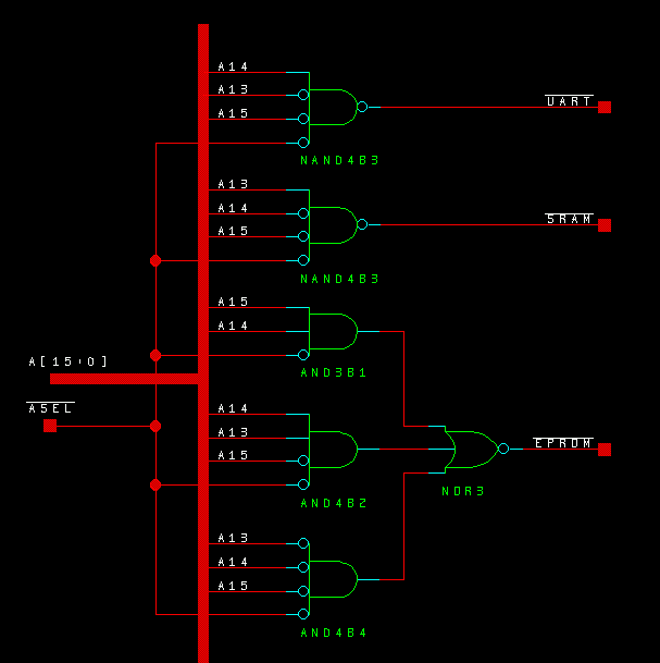
Address DecodeThis little circuit provides some simple address decoding, which would normally be implemented by a logic circuit on the circuit board. Because this design was implemented in a Xilinx FPGA chip, adding a bit of extra logic was easier than putting another chip on the board. The test board has three chips, a Flash ROM (which also contains the FPGA configuration bits), SRAM, and a UART.
|