Teensy 4.0 Development Board
SparkFun is now manufacturing Teensy products. You can buy directly at SparkFun.

|
TEENSY40_PINS | Teensy USB Board, Version 4.0, with Pins Soldered | $26.80 |
Teensy 4.0 is the latest Teensy, offering the fastest microcontroller and powerful peripherals in the Teensy 1.4 by 0.7 inch form factor.
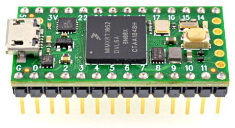
Teensy 4.0 can be programmed using the Arduino IDE with Teensyduino add-on.
Processor
Teensy 4.0 features an ARM Cortex-M7 processor at 600 MHz, with a NXP iMXRT1062 chip, the fastest microcontroller available today.

Benchmark results measured with CoreMark as an Arduino sketch. For an alterative to synthetic benchmarking, see this Digital Signature Speed Test.
Technical Specifications
- ARM Cortex-M7 at 600 MHz
- 1024K RAM (512K is tightly coupled)
- 2048K Flash (64K reserved for recovery & EEPROM emulation)
- 2 USB ports, both 480 MBit/sec
- 3 CAN Bus (1 with CAN FD)
- 2 I2S Digital Audio
- 1 S/PDIF Digital Audio
- 1 SDIO (4 bit) native SD
- 3 SPI, all with 16 word FIFO
- 3 I2C, all with 4 byte FIFO
- 7 Serial, all with 4 byte FIFO
- 32 general purpose DMA channels
- 31 PWM pins
- 40 digital pins, all interrrupt capable
- 14 analog pins, 2 ADCs on chip
- Cryptographic Acceleration
- Random Number Generator
- RTC for date/time
- Programmable FlexIO
- Pixel Processing Pipeline
- Peripheral cross triggering
- Power On/Off management
Pinouts
Teensy 4.0 is the same size and shape as Teensy 3.2, and retains compatibility with most of the pin functions on Teensy 3.2.


Power Consumption & Management
When running at 600 MHz, Teensy 4.0 consumes approximately 100 mA current.Teensy 4.0 provides support for dynamic clock scaling. Unlike traditional microcontrollers, where changing the clock speed causes wrong baud rates and other issues, Teensy 4.0 hardware and Teensyduino's software support for Arduino timing functions are designed to allow dynamically speed changes. Serial baud rates, audio streaming sample rates, and Arduino functions like delay() and millis(), and Teensyduino's extensions like IntervalTimer and elapsedMillis, continue to work properly while the CPU changes speed.
Teensy 4.0 also provides a power shut off feature. By connecting a pushbutton to the On/Off pin, the 3.3V power supply can be completely disabled by holding the button for 5 seconds, and turned back on by a brief button press. If a coin cell is connected to VBAT, Teensy 4.0's RTC also continues to keep track of date & time while the power is off.
Teensy 4.0 also can also be overclocked, well beyond 600 MHz!
Cortex-M7 Processor Details
ARM Cortex-M7 brings many powerful CPU features to a true real-time microcontroller platform.Cortex-M7 is a dual-issue superscaler processor, meaning M7 can execute 2 instructions per clock cycle, at 600 MHz! Of course, executing 2 simultaneously depends upon the compiler ordering instructions and registers. Initial benchmarks have shown C++ code compiled by Arduino tends to achieve 2 instructions about 40% to 50% of the time while performing numerically intensive work using integers and pointers.
Cortex-M7 is the first ARM microcontroller to use branch prediction. On M4, loops and other code which much branch take 3 clock cycles. With M7, after a loop has executed a few times, the branch prediction removes that overhead, allowing the branch instruction to run in only a single clock cycle.
Tightly Coupled Memory is a special feature which allows Cortex-M7 fast single cycle access to memory using a pair of 64 bit wide buses. The ITCM bus provides a 64 bit path to fetch instructions. The DTCM bus is actually a pair of 32 bit paths, allowing M7 to perform up to 2 separate memory accesses in the same cycle. These extremely high speed buses are separate from M7's main AXI bus, which accesses other memory and peripherals. 512K of memory can be accessed as tightly coupled memory. Teensyduino automatically allocates your Arduino sketch code into ITCM and all non-malloc memory use to the fast DTCM, unless you add extra keywords to override the optimized default.
Memory not accessed on the tightly coupled buses is optimized for DMA access by peripherals. Because the bulk of M7's memory access is done on the 2 tightly coupled buses, powerful DMA-based peripherals have excellent access to the non-TCM memory for highly efficient I/O.
Teensy 4.0's Cortex-M7 processor includes a floating point unit (FPU) which supports both 64 bit "double" and 32 bit "float". With M4's FPU on Teensy 3.5 & 36, and also Atmel SAMD51 chips, only 32 bit float is hardware accelerated. Any use of double, double functions like log(), sin(), cos() means slow software implemented math. Teensy 4.0 executes all of these with FPU hardware.
Memory Layout
Teensy 4.0 has 1 Mbyte of RAM and 2 Mbyte of Flash memory. The RAM is divided into 2 physically separate banks.
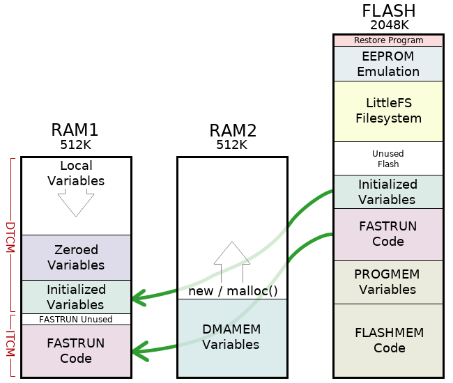
Memory is used in the following ways.
- Initialized Variables - These are global and static variables which have non-zero values defined. Their data is copied from Flash to RAM1 at startup.
- Zeroed Variables - These are all other global and static variables.
- Local Variables - Local variables, and also return addresses from function calls and the saved state from interrupts are placed on a stack which starts from the top of RAM1 and grown downward. The amount of space for local variable is the portion of RAM1 not used by FASTRUN code and the initialized and zeroed variables.
- DMAMEM Variables - Variables defined with "DMAMEM" are placed at the beginning of RAM2. Normally buffers and large arrays are placed here. These variables can not be initialized.
- PROGMEM Variables - Variables defined with "PROGMEM" are placed only in the flash memory. They can be accessed normally.
- new / malloc() - Memory allocated by C++ "new" and C malloc() comes from RAM2, starting immediately after the DMAMEM variables.
- FASTRUN Code - Functions defined with "FASTRUN" are allocated in the beginning of RAM1. A copy is also stored in Flash and copied to RAM1 at startup. These functions are accessed by the Cortex-M7 ITCM bus, for the fastest possible performance. By default, functions without any memory type defined are treated as FASTRUN. A small amount of memory is typically unused, because the ITCM bus must access a memory region which is a multiple of 32K.
- PROGMEM Code - Functions defined with "PROGMEM" executed directly from Flash. If the Cortex-M7 cache is not already holding a copy of the function, a delay results while the Flash memory is read into the M7's cache. PROGMEM should be used on startup code and other functions where speed is not important.
- EEPROM Emulation - 60K of Flash memory is reserved for EEPROM emulation. Normally the Arduino EEPROM library is used, but the AVR eeprom functions are also supported for compatibility with legacy code. During uploading, this portion of the Flash is not erased or altered, so your data saved in the "EEPROM" is retained.
- Restore Program - When you press the Teensy 4.0 pushbutton for 15 seconds (a quick flash on the red LED will tell you the moment to release), all of the Flash except this 4K is erased, and this known-good LED blink program is copied to the beginning of the Flash. This top 4K is special read-only memory, so you can always use this 15 second button press to fully erase your Teensy 4.0 and restore it to a known-good blink program.
TODO: add examples here of code using FASTRUN, PROGMEM, F(), DMAMEM
RAM1 is accessed by 2 extremely high speed 64 bit buses, ITCM for running code, and DTCM for accessing data. For the highest possible performance, place code and variables in RAM1. Caching is not used with RAM1, because all location in RAM1 are accessed at the same speed as the M7 processor's caches.
RAM2 is accessed by a 64 bit AXI bus which runs at 1/4 of the CPU clock speed. While slower than ITCM & DTCM, it is still very fast. Normally data buffers and large arrays are placed in RAM2. The ARM Cortex-M7 data cache is used with this memory. When DMA transfers are used, the data cache management functions must be used to flush or delete cached data. DMA from peripherals can access RAM2 without competing with the extremely high bandwidth usage of RAM1 by the ITCM & DTCM buses.
Flash is accessed by FlexSPI, which maps the entire Flash into the M7's memory. Any location in the Flash chip may be read as if it were ordinary memory. Caching is used, so often there is little performance loss. But a cache miss does require many clock cycles to fill a cache row from the Flash chip. Normally only large tables, startup code, and other resources which are not speed critical should be accessed from the Flash memory. String constants may be placed only in the flash using F("string") syntax.